Shanghai Fudan 01385.HK vs ASMPT 0522.HK: How to Distinguish Memory Chip Design from Advanced Packaging Equipment


If you are comparing Shanghai Fudan 01385.HK and ASMPT 0522.HK, the first thing to distinguish is “selling chips” versus “selling equipment.” Shanghai Fudan is more like a multi-product IC design company, with businesses covering FPGA, non-volatile memory, security chips, smart meter chips, and testing services. ASMPT is more like a semiconductor packaging and electronics manufacturing equipment company, with advanced packaging, TCB, Hybrid Bonding, HBM, and CPO as key clues. The former depends more on chip product shipments and domestic substitution, while the latter depends more on packaging equipment orders and AI/HBM capital expenditure.
Key Takeaways
- Shanghai Fudan is closer to chip design, while ASMPT is closer to packaging equipment.
- Shanghai Fudan’s memory exposure comes from EEPROM, NOR Flash, and SLC NAND.
- ASMPT’s AI exposure mainly comes from TCB, HB, HBM, and CPO.
- Shanghai Fudan is more affected by domestic substitution, FPGA, and niche memory demand.
- ASMPT is more affected by advanced packaging expansion and AI chip capital expenditure.
- The first step in comparing them is to identify whether revenue comes from chips or equipment.
Where Do Shanghai Fudan and ASMPT Sit in the Semiconductor Supply Chain?
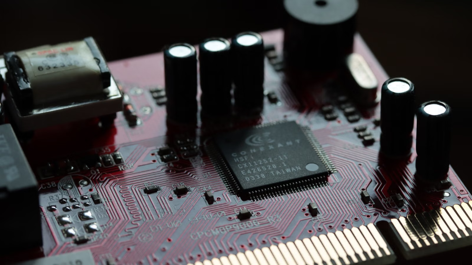
Shanghai Fudan and ASMPT are both related to semiconductors, but they are not the same type of company. Shanghai Fudan 01385.HK is closer to chip design and chip product sales, with revenue coming from FPGA, non-volatile memory, security identification chips, MCU products, and testing services. ASMPT 0522.HK is closer to semiconductor manufacturing equipment, with revenue coming from packaging, assembly, SMT, and advanced packaging equipment. You can think of Shanghai Fudan as a company that designs and sells chips, while ASMPT provides equipment for chip manufacturing and packaging.
Shanghai Fudan disclosed in its 2025 annual report that its major product lines include FPGA, security and identification chips, non-volatile memory, smart meter chips, and integrated circuit testing services through Hualing. Its FPGA and other product revenue was about RMB 1.42 billion, while non-volatile memory revenue was about RMB 1.04 billion. It is not a DRAM, HBM, or large-capacity 3D NAND manufacturer, but a multi-product domestic IC design company.
ASMPT has a completely different position. In its 2025 annual results, the company described itself as a semiconductor and electronics manufacturing hardware and software solutions provider, with businesses covering Semiconductor Solutions and SMT Solutions. Its relationship with HBM, AI chips, and advanced logic is not that it produces memory chips, but that it provides TCB, Hybrid Bonding, die bonding, wire bonding, SMT, and related equipment and process solutions.
| Dimension | Shanghai Fudan 01385.HK | ASMPT 0522.HK |
|---|---|---|
| Supply chain position | Chip design and product sales | Semiconductor packaging and electronics manufacturing equipment |
| Core businesses | FPGA, non-volatile memory, security chips, MCU | TCB, HB, die bonding, wire bonding, SMT |
| Memory exposure | EEPROM, NOR Flash, SLC NAND | HBM advanced packaging equipment |
| AI exposure | FPGA, FPAI, edge AI, data processing | AI chips, HBM, CPO, advanced packaging |
| Key metrics | Product revenue, gross margin, R&D conversion | Orders, backlog, equipment delivery, gross margin |
Summary: The biggest difference between Shanghai Fudan and ASMPT is the difference between a chip product company and an equipment company. Shanghai Fudan’s core lies in IC design, FPGA, non-volatile memory, and domestic substitution, so its performance is more affected by product ramp-up, customer validation, R&D investment, and downstream applications. ASMPT’s core lies in semiconductor packaging equipment and electronics manufacturing equipment, so its performance is more affected by AI chips, HBM, CPO, OSAT/IDM customer capital expenditure, and equipment orders. Both companies belong to the semiconductor supply chain, but they should not be compared under the same simple “memory stock” label.
What Does Shanghai Fudan’s “Memory Chip Design” Actually Mean?
Shanghai Fudan’s memory chip business mainly refers to EEPROM, NOR Flash, SLC NAND, and other non-volatile memory products, rather than DRAM, HBM, or server-grade high-capacity NAND. Non-volatile memory can retain data even after power is cut off, and is commonly used in automotive electronics, industrial control, communications, security, smart meters, and consumer electronics. Its logic is closer to niche memory, embedded storage, and domestic substitution, so it should not be analyzed directly with the global HBM or DRAM cycle framework.
Shanghai Fudan’s non-volatile memory products cover EEPROM, SPI NOR Flash, and NAND Flash. Company materials show that its EEPROM products cover 1Kbit to 4096Kbit, SPI NOR Flash covers 0.5Mbit to 1Gbit, and NAND Flash covers 0.5Gbit to 8Gbit. Its English materials show that SLC NAND Flash products cover 0.5Gbit to 8Gbit, with applications in communication equipment, set-top boxes, network products, toys, and other devices.
The value of these storage products does not come from having the largest capacity, but from reliability, interface compatibility, industrial-grade usage, customer qualification, and domestic substitution. For example, automotive EEPROM, industrial NOR Flash, and SLC NAND used in security or networking equipment usually require stable supply, long product lifecycles, and specific scenario adaptation. This is very different from the high-bandwidth memory logic of HBM, and it is also different from the price cycle of consumer high-capacity NAND.
However, Shanghai Fudan’s growth story is not only about memory. In its company profile, the company says that its FPGA products are used in communications, artificial intelligence, industrial control, signal processing, and other fields, and that it has developed FPAI chips for AI applications. Its 2026 exhibition materials also mentioned the new-generation heterogeneous reconfigurable intelligent chip FMZQ400TAI, with peak AI performance of 128TOPS@INT8, targeting edge AI, industrial vision, medical imaging, and other scenarios.
You can judge Shanghai Fudan’s memory exposure through five points:
- Whether the related products come from EEPROM, NOR Flash, or SLC NAND;
- Whether these products belong to non-volatile and niche memory;
- Whether downstream applications include automotive, industrial, communications, security, or IoT;
- Whether growth comes from domestic substitution, customer qualification, and product iteration;
- Whether you have separated it from HBM, DRAM, and mainstream 3D NAND.
Summary: Shanghai Fudan does have memory chip products, but its more accurate positioning is “niche non-volatile memory + FPGA + multi-product IC design company.” Its EEPROM, NOR Flash, and SLC NAND products target embedded, industrial, automotive, communications, and security scenarios, not the same track as HBM, DRAM, or high-capacity NAND manufacturers. If you follow Shanghai Fudan, you should look at non-volatile memory, FPGA, FPAI, R&D investment, customer qualification, and domestic substitution progress together, rather than simply treating it as a “memory chip stock.”
What Does ASMPT’s “Advanced Packaging Equipment” Actually Mean?
ASMPT’s advanced packaging equipment refers to equipment and solutions used for chip assembly, packaging, interconnect, and electronics manufacturing. It does not design HBM, nor does it sell FPGA or NOR Flash. Instead, it provides packaging equipment for AI chips, HBM, chiplets, CPO, advanced logic, and SiP. When analyzing ASMPT, the key is not how many chips a single product sells, but whether customers are expanding capacity, whether TCB/HB orders are increasing, and whether equipment delivery is progressing smoothly.
TCB stands for Thermo-Compression Bonding. AI chips and HBM packaging increasingly require high-density interconnects, smaller pitch, better thermal management, and higher yield, while traditional packaging processes cannot fully meet these requirements. ASMPT disclosed in its 2025 results that advanced packaging revenue reached US$532.1 million, up 30.2% year on year; TCB revenue increased by about 146%, and the company expects the TCB TAM to grow from about US$760 million in 2025 to US$1.6 billion in 2028.
HBM is a key concept for understanding ASMPT, but its role must be stated clearly. ASMPT does not produce HBM chips; it provides equipment for HBM stacking, interconnect, and packaging. The company said its TCB solutions had received multiple customer orders for HBM4 12H and that it was advancing HBM4 16H technology development. In the first quarter of 2026, ASMPT also said its TCB and HB solutions support next-generation AI compute and HBM, while Photonics and CPO support high-speed data demand.
| Advanced Packaging Concept | Relationship with ASMPT | Meaning for AI/HBM |
|---|---|---|
| TCB | One of its core equipment solutions | Supports high-density interconnects for advanced logic and HBM |
| Hybrid Bonding | Next-generation bonding tool | Improves interconnect density and performance |
| C2S / C2W | Advanced packaging process directions | Used for chip-to-substrate and chip-to-wafer connections |
| HBM | ASMPT does not produce HBM | Provides equipment for HBM packaging and stacking |
| CPO / Photonics | Related to high-speed data transmission | Supports AI data center network upgrades |
| SMT | Electronics manufacturing assembly solution | Supports AI servers and high-density board assembly |
The cycle of an equipment company is also different from that of a chip design company. ASMPT’s revenue comes from equipment purchases by OSATs, IDMs, packaging houses, and electronics manufacturing customers. When AI chips, HBM, CPO, SiP, and advanced logic expand capacity, equipment orders rise. When customers slow capital expenditure, orders, backlog, and revenue recognition may come under pressure. ASMPT’s first-quarter 2026 HK$5.67 billion bookings reflected this equipment order cycle.
Summary: ASMPT’s advanced packaging equipment nature makes it closer to AI chip manufacturing upgrades, not memory chip design. Its core variables are TCB, Hybrid Bonding, die bonding, wire bonding, CPO, SMT, and customer capital expenditure. If you care about HBM stacking, advanced logic packaging, chiplets, and AI server hardware manufacturing, ASMPT has more direct exposure. But this type of equipment stock is also affected by order timing, customer CAPEX, technology roadmaps, and delivery cycles, so it should not be judged only by the AI theme.
How Are the Benefit Chains Different If Both Companies Are Related to AI and Memory?
Shanghai Fudan’s AI/memory exposure is more like “end-market demand driving chip shipments,” while ASMPT’s AI/HBM exposure is more like “manufacturing upgrades driving equipment orders.” This is a critical dividing line. When Shanghai Fudan benefits, it usually appears as improved shipments of FPGA, non-volatile memory, security chips, and other products. When ASMPT benefits, it usually appears as higher orders for TCB, HB, die bonding, wire bonding, SMT, and other equipment. The former depends on product competitiveness, while the latter depends on the capital expenditure cycle.
Shanghai Fudan’s transmission path is: AIoT, automotive electronics, industrial control, communications, data centers, and high-reliability applications grow, driving demand for EEPROM, NOR Flash, SLC NAND, FPGA, and FPAI, which then shows up in product revenue, gross margin, and customer mix. It is better analyzed through the framework of product line revenue, R&D conversion, domestic substitution, and customer qualification.
ASMPT’s transmission path is: AI chips, HBM, advanced logic, CPO, and high-density AI server boards expand capacity, prompting OSATs, IDMs, packaging houses, and electronics manufacturers to buy equipment, which then appears as bookings, backlog, equipment delivery, and revenue recognition. In its nineteen C2S TCB tool orders, ASMPT stated that its TCB installed base exceeded 500 units and was positioned for the expansion of the AI chip market.
| Comparison Dimension | Shanghai Fudan | ASMPT |
|---|---|---|
| Demand starting point | End-market chip demand | Advanced packaging capacity expansion |
| Revenue source | Chip product sales, testing services | Equipment sales, solutions, and services |
| AI transmission path | Edge AI, AIoT, data processing chips | AI chip manufacturing, HBM packaging, CPO |
| Main customers | Industrial, communications, automotive, electronics customers | OSATs, IDMs, packaging houses, electronics manufacturers |
| Key metrics | Product revenue, gross margin, R&D conversion | Orders, backlog, delivery, equipment penetration |
This also determines the different risks each company faces. Shanghai Fudan needs to keep proving that its products can be adopted by customers, especially whether FPGA, FPAI, and high-reliability memory products can move from R&D into scaled revenue. ASMPT needs to prove that advanced packaging equipment demand can continue to be released, especially whether TCB, HB, CPO, and AI server SMT demand can withstand changes in customer expansion cycles.
Summary: Although both companies are related to AI and memory, Shanghai Fudan and ASMPT have completely different benefit chains. Shanghai Fudan is more like a product company, with the core lying in chip design, product iteration, customer qualification, and domestic substitution realization. ASMPT is more like an equipment company, with the core lying in advanced packaging expansion, equipment orders, customer CAPEX, and delivery timing. When comparing the two, you should not only ask “which one is more like a semiconductor stock,” but first clarify whether you are looking at improving end-market chip demand or the manufacturing equipment upgrade cycle.
How Should You Compare Shanghai Fudan and ASMPT by Financial Leverage, Cyclicality, and Risk?
If you focus on domestic substitution in chip design and niche memory, Shanghai Fudan is more suitable for observation. If you focus on AI/HBM advanced packaging expansion, ASMPT has more direct exposure. Shanghai Fudan’s financial leverage comes from product mix, shipments, gross margin, and R&D conversion. ASMPT’s financial leverage comes from equipment orders, backlog, customer capital expenditure, and advanced packaging penetration. Both are affected by the semiconductor cycle, but their triggers are different.
Shanghai Fudan’s 2025 revenue increased year on year, but profit came under pressure. Its annual report disclosed 2025 revenue of about RMB 3.98 billion, up 10.92% year on year, while net profit attributable to shareholders was about RMB 232 million, down 59.42% year on year. This shows that even if a chip design company grows revenue, product pricing, gross margin, R&D investment, expenses, and competition can still affect profit conversion.
ASMPT’s leverage comes more from equipment orders. The company reported HK$13.74 billion revenue for 2025, up 10.0% year on year, and group bookings of HK$14.48 billion, up 21.7%. In the first quarter of 2026, ASMPT reported revenue of HK$3.97 billion, a book-to-bill ratio of 1.43, and second-quarter revenue guidance of US$540 million to US$600 million. These indicators are more suitable for an equipment company, because orders and delivery cadence often lead revenue recognition.
| Comparison Dimension | Shanghai Fudan 01385.HK | ASMPT 0522.HK |
|---|---|---|
| Source of financial leverage | Chip product ramp-up, product mix improvement | Advanced packaging equipment order growth |
| Cyclical nature | Chip design and downstream demand cycle | Semiconductor equipment capital expenditure cycle |
| Main risks | Niche memory pricing, R&D expenses, qualification cycles | Order delays, CAPEX slowdown, technology roadmap changes |
| AI directness | Moderate, more edge AI and chip applications | More direct, focused on HBM/AI chip manufacturing |
| Valuation framework | Domestic IC design + FPGA + niche memory | Advanced packaging equipment + AI/HBM CAPEX |
If you plan to follow 01385.HK, 0522.HK, or other Hong Kong-listed semiconductor names, you should also include trading costs and cross-market risk in the comparison framework. Cross-market trading does not only involve commissions; it may also involve platform fees, external institution fees, transaction activity fees, FX changes, order types, and market rules. When using Biya to view related stocks, you can also check quotes, order details, and fee structure. Biya charges US$0 commission for U.S. stock trading, while platform fees, external institution fees, and other charges are subject to the U.S. stock trading fees and the actual order page; Hong Kong stock and other market fees should be subject to the platform display and applicable market rules.
Summary: Shanghai Fudan and ASMPT both have semiconductor cycle exposure, but they should not be evaluated with the same valuation and tracking indicators. Shanghai Fudan is better observed through IC design, FPGA, non-volatile memory, domestic substitution, and R&D conversion. ASMPT is better observed through advanced packaging equipment, TCB/HB, AI/HBM capital expenditure, orders, and backlog. If you care more about product competitiveness, Shanghai Fudan is more relevant. If you care more about manufacturing upgrades and equipment expansion, ASMPT is more direct.
Final Judgment: How Do You Distinguish Memory Chip Design from Advanced Packaging Equipment?
The simplest way to distinguish memory chip design from advanced packaging equipment is to look at where revenue comes from. Shanghai Fudan sells chip products and testing services, including FPGA, EEPROM, NOR Flash, SLC NAND, security chips, and MCU products. ASMPT sells equipment and solutions for packaging, assembly, SMT, TCB, Hybrid Bonding, die bonding, and wire bonding. The former depends on chip product demand, while the latter depends on customer capacity expansion and equipment orders.
The second dimension is the AI/HBM transmission path. Shanghai Fudan’s relationship with AI mainly comes from FPGA, FPAI, edge AI, AIoT, data processing, and niche memory applications. ASMPT’s relationship with AI/HBM mainly comes from advanced packaging equipment, especially TCB, HB, C2S/C2W, CPO, and AI server hardware manufacturing. If the question is “who benefits more directly from HBM packaging expansion,” ASMPT is the clearer answer. If the question is “who benefits more from domestic chip design and niche memory,” Shanghai Fudan is clearer.
The third dimension is risk source. Shanghai Fudan requires attention to product pricing, customer qualification, R&D investment, domestic substitution progress, and product iteration. ASMPT requires attention to equipment orders, customer CAPEX, delivery cycles, technology roadmap changes, and advanced packaging penetration. Ordinary investors should first judge whether they understand the product cycle or the equipment cycle.
| Key Question | More Shanghai Fudan | More ASMPT |
|---|---|---|
| Which one is a chip design company? | Yes | No |
| Which one is closer to advanced packaging equipment? | No | Yes |
| Which one is more related to niche memory? | Yes | Indirect |
| Which one is more related to HBM packaging expansion? | Indirect | Yes |
| Which one depends more on end-market chip demand? | Yes | Partly |
| Which one depends more on equipment orders and CAPEX? | Partly | Yes |
The final conclusion is straightforward: Shanghai Fudan represents the logic of “chip design/product sales,” while ASMPT represents the logic of “advanced packaging/equipment sales.” Shanghai Fudan is better placed in the framework of domestic IC design, FPGA, non-volatile memory, and edge AI. ASMPT is better placed in the framework of AI chips, HBM, advanced packaging equipment, and semiconductor capital expenditure. Both companies may benefit from semiconductor upcycles, but their indicators, cycles, and risks are different.
Summary: The core difference between memory chip design and advanced packaging equipment is not that both are in the semiconductor industry, but that one sells chips while the other sells equipment. Shanghai Fudan’s core variables are product capability, customer qualification, R&D conversion, niche memory, and domestic substitution. ASMPT’s core variables are TCB/HB orders, advanced packaging expansion, AI/HBM capital expenditure, and delivery timing. If you want to compare 01385.HK and 0522.HK, first place both companies in the correct supply chain position, then discuss valuation, earnings leverage, and risk tolerance.
When comparing Shanghai Fudan and ASMPT, you can use U.S. stock information to extend your tracking to global semiconductor, memory chip, AI equipment, and advanced packaging companies, while also observing Hong Kong-listed supply chain names such as 01385.HK and 0522.HK. If the relevant services are available in your region, Biya can help you check quotes, orders, and multi-asset trading arrangements. For mobile use, Download App can support account, order, and asset tracking. The information above only discusses public market data, company financial reports, and supply chain differences. It does not constitute investment advice. Before trading, you should fully understand order types, fee structures, FX changes, tax requirements, and your own risk tolerance. Service availability depends on your location, identity verification result, platform rules, and applicable laws and regulations.
FAQ
Is Shanghai Fudan 01385.HK a Memory Chip Stock?
It is memory-related, but more accurately, it is a multi-product IC design company. Its memory exposure mainly comes from non-volatile memory products such as EEPROM, NOR Flash, and SLC NAND. It is not the same as a DRAM, HBM, or high-capacity NAND manufacturer.
Is ASMPT 0522.HK an Advanced Packaging Equipment Stock?
Yes. ASMPT is better classified as a semiconductor packaging equipment and SMT solutions company. Its relationship with AI and HBM mainly comes from advanced packaging equipment such as TCB, Hybrid Bonding, die bonding, wire bonding, and CPO.
Which Benefits More from the HBM Supply Chain, Shanghai Fudan or ASMPT?
If you focus only on HBM packaging expansion, ASMPT has more direct exposure, because TCB and Hybrid Bonding equipment are related to HBM stacking and interconnects. Shanghai Fudan’s HBM exposure is more indirect, with more focus on niche memory, FPGA, and chip design.
What Is the Difference Between Memory Chip Design and Advanced Packaging Equipment?
Memory chip design companies mainly design and sell chip products, with revenue coming from chip shipments and product mix. Advanced packaging equipment companies sell equipment to packaging houses, IDMs, or OSATs, so their revenue is more affected by customer capital expenditure and equipment orders.
What Metrics Should Investors Track When Comparing Shanghai Fudan and ASMPT?
For Shanghai Fudan, investors should track FPGA revenue, non-volatile memory revenue, gross margin, R&D investment, and customer qualification. For ASMPT, investors should track advanced packaging revenue, TCB/HB orders, backlog, delivery cadence, and semiconductor equipment capital expenditure.
*This article is provided for general information purposes and does not constitute legal, tax or other professional advice from BiyaPay or its subsidiaries and its affiliates, and it is not intended as a substitute for obtaining advice from a financial advisor or any other professional.
We make no representations, warranties or warranties, express or implied, as to the accuracy, completeness or timeliness of the contents of this publication.
Related Blogs of

HBM/DRAM, NAND, and HDD in AI Storage: A Comparison of Elasticity, Cycles, and Risks


How to Read Pure Storage and NetApp Earnings? ARR, Cloud Revenue, Gross Margin, and Cash Flow Metrics


How Is China’s Memory Supply Chain Different from Overseas Memory Leaders? A Comparison with Micron, SanDisk, Western Digital, and Seagate


How Does NAND Price Increase Affect SanDisk? Enterprise SSDs, Consumer Storage, and Margin Leverage

Choose Country or Region to Read Local Blog

Contact Us


BIYA GLOBAL LLC is registered with the Financial Crimes Enforcement Network (FinCEN), an agency under the U.S. Department of the Treasury, as a Money Services Business (MSB), with registration number 31000218637349, and regulated by the Financial Crimes Enforcement Network (FinCEN).
BIYA GLOBAL LIMITED is a registered Financial Service Provider (FSP) in New Zealand, with registration number FSP1007221, and is also a registered member of the Financial Services Complaints Limited (FSCL), an independent dispute resolution scheme in New Zealand.