What Is the Relationship Between ASMPT 0522.HK and HBM? The Role of Advanced Packaging Equipment in the AI Memory Supply Chain


The relationship between ASMPT 0522.HK and HBM is not that ASMPT “produces high-bandwidth memory,” but that it provides equipment capabilities needed for advanced packaging of HBM and AI chips. HBM must be integrated with GPUs, ASICs, or AI accelerators through stacking, bonding, micro-bumps, silicon interposers, and 2.5D/3D packaging to achieve high-bandwidth and low-power interconnects. ASMPT’s investment logic mainly comes from back-end equipment orders such as TCB, Flip Chip, Hybrid Bonding, and Die Bonding, rather than DRAM chip shipments.
Key Takeaways
- ASMPT is not an HBM manufacturer, but an advanced packaging equipment supplier.
- HBM requires packaging equipment for stacking, bonding, placement, and interconnection.
- TCB, Flip Chip, and Hybrid Bonding are key terms for understanding 0522.HK.
- AI compute demand is transmitted to ASMPT through packaging capacity expansion.
- ASMPT should be evaluated by orders, margins, delivery, SMT cycles, and valuation.
What Exactly Is the Relationship Between ASMPT 0522.HK and HBM?

The relationship between ASMPT 0522.HK and HBM is an advanced packaging equipment supply relationship, not a memory chip manufacturing relationship. HBM is produced by memory companies such as Samsung, SK Hynix, and Micron, while ASMPT’s role is closer to that of an equipment supplier that helps assemble chips into packaging systems with high precision. In AI server and high-performance computing scenarios, HBM must work together with GPUs, ASICs, chiplets, silicon interposers, and package substrates. Advanced packaging equipment is the key tool that connects these components.
ASMPT is a Hong Kong-listed company whose businesses cover semiconductor assembly and packaging equipment, SMT surface-mount technology equipment, and related automation solutions. It should be positioned in back-end semiconductor equipment, rather than memory chip manufacturing. In its 2025 annual results, the company stated that TCB revenue reached a record high, up about 146% year over year, and raised its TCB total addressable market forecast from about USD 760 million in 2025 to about USD 1.6 billion in 2028. The growth drivers include advanced logic and HBM applications.
| HBM Supply Chain Segment | Representative Company Type | Does ASMPT Directly Participate? | Meaning for 0522.HK |
|---|---|---|---|
| HBM DRAM manufacturing | SK Hynix, Samsung, Micron | No | It does not earn revenue from memory chip shipments |
| Logic chip manufacturing | Foundries, IDMs | No | It is indirectly affected by AI chip demand |
| Advanced packaging services | Foundries, OSATs | Indirectly related | Packaging expansion creates equipment demand |
| TCB / Die Bonding / Flip Chip | Back-end packaging equipment makers | Yes | This is ASMPT’s key beneficiary segment |
| SMT electronics assembly | EMS and terminal manufacturing chains | Yes | It affects ASMPT’s overall revenue cycle |
This also explains why ASMPT is often included in the HBM supply chain, but should not be confused with HBM memory manufacturers. The core variables for HBM makers are DRAM capacity, yield, customer qualification, and HBM3E / HBM4 product iteration. The core variables for ASMPT are advanced packaging customer expansion, equipment orders, delivery cycles, acceptance timing, gross margin, and market share.
In its 2026 first-quarter results, ASMPT continued to emphasize AI-driven demand for advanced packaging, including TCB, Hybrid Bonding, Photonics, and CPO. This shows that 0522.HK’s AI memory logic comes from equipment capital expenditure, not from HBM price increases themselves. The more complex HBM becomes, the more precise packaging must be, and the larger AI chip packages become, the more important back-end equipment becomes. However, equipment orders usually lag terminal demand and customer expansion plans.
Summary: ASMPT has a clear relationship with HBM, but that relationship sits at the advanced packaging equipment layer. It does not produce HBM, participate in DRAM wafer manufacturing, or make GPUs. The core logic for 0522.HK is that AI compute demand drives HBM and advanced packaging capacity expansion, packaging customers need more TCB, Flip Chip, Die Bonding, and Hybrid Bonding equipment, and ASMPT may therefore receive order and revenue opportunities. When evaluating the company, focus on equipment orders, delivery, customer expansion, and the revenue share of advanced packaging.
Why Can HBM Not Work Without Advanced Packaging Equipment?
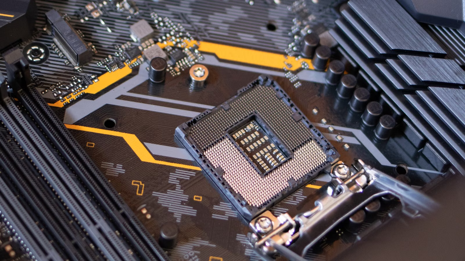
HBM cannot work without advanced packaging because it is not a standalone memory chip, but a high-bandwidth memory system formed by stacking multiple DRAM dies through TSVs, micro-bumps, bonding, and package substrates. AI accelerators need to place HBM close to GPUs or ASICs, using 2.5D packaging and silicon interposers to shorten signal paths, increase bandwidth, and reduce power consumption. Without advanced packaging, HBM’s high-bandwidth advantage would be difficult to convert into actual AI training and inference performance.
The basic logic of HBM is “stacking” and “proximity to compute.” Traditional memory connects to CPUs or GPUs across longer distances, which can create bandwidth bottlenecks and power-consumption pressure. HBM vertically stacks multiple DRAM layers, connects them through TSVs, and places them in the same packaging system as compute chips. As the HBM4 standard advances, bandwidth, capacity, power efficiency, and packaging complexity continue to rise, making packaging equipment capability an increasingly important supply-chain constraint.
TSMC’s CoWoS is one of the key process platforms for understanding HBM. CoWoS-S uses silicon interposers to enable high-density interconnection and can accommodate logic chiplets and HBM cubes on a large interposer, targeting high-performance computing applications such as AI and supercomputing. In other words, HBM’s value does not come only from the memory dies, but from the system formed together with GPUs, ASICs, package substrates, and silicon interposers.
| Key Packaging Step | Technical Keywords | Equipment Demand | Supply Chain Impact |
|---|---|---|---|
| DRAM die stacking | TSV, micro-bump | High-precision bonding, alignment, inspection | Determines HBM yield and bandwidth |
| HBM and logic chip integration | 2.5D, CoWoS, interposer | Die Bonding, Flip Chip, TCB | Affects AI chip delivery capacity |
| Chiplet connection | Heterogeneous Integration | High-precision placement, thermo-compression bonding | Drives demand for advanced packaging equipment |
| Finer-pitch interconnects | Hybrid Bonding | D2W, W2W, ultra-high-precision bonding | Points to next-generation packaging routes |
The larger AI chips become, the harder packaging becomes. Multiple HBM stacks must be placed around GPUs or ASICs. Data bandwidth, thermal management, warpage control, placement accuracy, yield, and testing all become part of the system engineering challenge. Advanced packaging bottlenecks often appear not only at one foundry, but also in equipment delivery, packaging line ramp-up, packaging materials, substrate supply, and customer qualification cycles.
This is where ASMPT’s value enters. It does not determine HBM chip pricing, but it may influence whether packaging customers can complete high-end AI packages on time and at acceptable yields. As AI server demand rises, supply-chain expansion no longer depends only on EUV, advanced nodes, and DRAM wafers. It also depends on CoWoS, TCB, Hybrid Bonding, packaging and testing, and back-end equipment supply.
Summary: HBM is not an ordinary memory module. It is a 3D-stacked memory system designed for high bandwidth, low power, and near-compute integration. It requires advanced packaging to connect multiple DRAM layers, logic chips, silicon interposers, and substrates. The value of advanced packaging equipment lies in improving placement accuracy, bonding quality, interconnect density, and mass-production yield. Therefore, ASMPT’s connection to HBM is not in memory manufacturing, but in AI chip packaging capacity expansion and high-precision back-end equipment demand.
Where Do ASMPT’s TCB, Flip Chip, and Hybrid Bonding Fit?

ASMPT’s key value in the HBM and AI packaging chain lies in high-precision placement and bonding equipment. TCB performs thermo-compression bonding and is suitable for high-end chiplets, HBM, and advanced logic packaging. Flip Chip is used for inverted chip connection and precision placement in 2.5D packaging. Hybrid Bonding targets finer pitch and higher-density interconnects, making it an important direction for next-generation 3D integration. These terms may sound complex, but they all point to the same essential task: connecting chips more accurately, more densely, and more reliably.
TCB is the most important keyword in ASMPT’s relationship with HBM today. TCB, or Thermo-Compression Bonding, uses temperature, pressure, and precise alignment to bond chips to substrates, chips to wafers, or chips to chips. ASMPT’s FIREBIRD TCB is described as a thermo-compression bonding system for 2D, 2.5D, and 3D heterogeneous integration, suitable for high-performance computing and AI applications. The company’s materials also mention placement accuracy of up to ±2.0 μm and emphasize high precision and production efficiency.
Flip Chip can be understood as “mounting the chip upside down.” Compared with traditional wire bonding, flip chip connects the die to the substrate through bumps, shortening signal paths and increasing I/O density. It is more suitable for high-performance chip packaging. In its 2026 first-quarter results, ASMPT noted that 2.5D packaging is being rapidly adopted in larger AI packages, driving orders for FC solutions in embedded bridge die bonding. For investors, the meaning of Flip Chip is that as AI chip packages become larger and interconnect requirements increase, demand for higher-precision placement equipment may rise.
Hybrid Bonding represents a more advanced interconnect direction. It is usually used for finer-pitch and higher-density chip connections, can reduce bump size or enable copper-to-copper bonding, and is drawing attention in next-generation HBM, chiplets, and 3D stacking. ASMPT has referred to HB solutions in several advanced packaging scenarios and has showcased platform capabilities for AI accelerators, HBM integration, and chiplet heterogeneous architectures at technical events such as ECTC.
| Technology | Simplified Explanation | Packaging Scenario | ASMPT Relevance | Investment Indicator |
|---|---|---|---|---|
| TCB | High-precision bonding using heat and pressure | HBM, chiplets, 2.5D/3D | High | Orders, installed base, revenue growth |
| Flip Chip | High-density inverted chip connection | AI large packages, bridge dies | High | FC orders and packaging customer expansion |
| Hybrid Bonding | Finer-pitch, high-density interconnects | Next-generation 3D integration | Medium to high | Technical validation, customer adoption |
| Die Bonding | Basic chip placement capability | Broad semiconductor packaging steps | High | Equipment accuracy and customer coverage |
In its 19-unit Chip-to-Substrate TCB tool order, ASMPT stated that its technology portfolio covers chip-on-wafer, chip-on-substrate, and HBM applications. It later disclosed 15 additional Chip-to-Substrate TCB tool orders driven by AI demand. These orders are more meaningful than broad industry concepts because they directly reflect customer expansion intentions.
Summary: TCB, Flip Chip, and Hybrid Bonding are the key technology gateways through which ASMPT enters the HBM and AI packaging chain. TCB corresponds to high-end thermo-compression bonding, Flip Chip corresponds to inverted chip placement and 2.5D packaging, while Hybrid Bonding points to future higher-density interconnects. For 0522.HK, technical terms ultimately need to translate into orders, delivery, installed base, revenue, and margins. Only when advanced packaging equipment demand continues to materialize can the HBM logic be reflected in company performance.
How Does AI Compute Demand Translate into ASMPT Orders and Revenue?
AI compute demand does not directly become ASMPT revenue. It first becomes demand for GPUs, ASICs, HBM, and advanced packaging expansion, then flows through foundries, OSATs, IDMs, and packaging customers’ capital expenditure into equipment orders. This process has a time lag. Rising training and inference demand drives AI chip orders. AI chips require HBM and 2.5D/3D packaging. When packaging capacity is insufficient, customers purchase equipment such as TCB, Flip Chip, and Die Bonding tools. Only after equipment delivery, installation, tuning, and acceptance does the order convert into revenue for ASMPT.
The transmission chain can be divided into six steps:
- Large-model training and inference increase compute demand.
- Cloud providers and AI companies increase GPU / ASIC purchases.
- AI chips drive demand for HBM, CoWoS, and 2.5D packaging.
- Foundries, OSATs, and IDMs expand advanced packaging capacity.
- Packaging customers purchase TCB, FC, HB, and Die Bonding equipment.
- ASMPT converts orders into revenue through delivery and acceptance.
The key to this chain is that packaging capacity has become an important variable in AI chip delivery. TrendForce has described AI competition as a supply-chain-level arms race, with advanced packaging and advanced-node capacity becoming important constraints. For ASMPT, this means it is not an end AI application company, nor a GPU company, but a form of “equipment leverage” behind compute capacity expansion.
However, equipment companies differ significantly from chip companies. HBM manufacturers may show direct revenue sensitivity through shipments, selling prices, and yield. ASMPT’s revenue depends more on equipment order cycles. After customers place orders, tools must be manufactured, shipped, installed, adjusted, and accepted. Revenue recognition may therefore lag. Order growth is a leading signal; revenue and gross margin are the confirmation signals.
Cyclical risks also come from this structure. If AI capital expenditure slows after a period of overheating, or if customers have already pulled equipment purchases forward, new orders may decline for a period. If packaging customers delay capacity expansion, equipment delivery can be affected. If technology routes change, such as faster adoption of different bonding equipment, the existing product portfolio must continue to evolve. ASMPT’s SMT business is also affected by cycles in consumer electronics, automotive electronics, and industrial electronics, so it cannot be evaluated only through advanced packaging.
Summary: AI compute demand reaches ASMPT through multiple layers: GPU / ASIC demand, HBM demand, advanced packaging demand, customer capacity expansion, equipment procurement, and delivery acceptance. ASMPT is an indirect beneficiary, not a linear or synchronous beneficiary. Order growth can indicate improving industry conditions earlier, but revenue, margins, and cash flow show whether the HBM logic has actually materialized. When analyzing 0522.HK, pay attention to both AI expansion intensity and equipment delivery cycles.
How Is ASMPT Different from Other HBM Supply Chain Companies?
ASMPT differs from companies such as SK Hynix, Micron, Samsung, TSMC, ASE, and Amkor because it is not an HBM memory producer, foundry, or outsourced packaging and testing service provider. It is a packaging and assembly equipment supplier. It does not earn the product price of each HBM chip or the service fee from CoWoS packaging. It earns money when customers expand capacity and purchase equipment. Therefore, the valuation logic of 0522.HK is closer to a semiconductor equipment stock than a memory chip stock.
Compared with HBM manufacturers, ASMPT does not directly bear the risks of DRAM wafer manufacturing, HBM die stacking product qualification, or memory contract price fluctuations. The core indicators for SK Hynix, Micron, and Samsung include HBM3E / HBM4 yield, capacity allocation, customer qualification, ASP, and long-term supply agreements. Micron’s High-bandwidth memory product line emphasizes that HBM targets high-performance, high-bandwidth workloads, and this type of business is directly reflected in memory product revenue.
Compared with foundries such as TSMC, ASMPT does not provide full CoWoS packaging services. TSMC is responsible for advanced process nodes, wafer manufacturing, and part of the advanced packaging platform. When CoWoS capacity is tight, foundries directly benefit from packaging service demand. ASMPT’s role is to provide part of the equipment capability to this ecosystem, making it an upstream tool supplier.
Compared with OSATs such as ASE and Amkor, ASMPT is also not the packaging and testing capacity itself. OSATs receive packaging and testing orders from customers and purchase equipment when they expand capacity. ASMPT sells equipment to packaging plants and related customers. The advantage of an equipment supplier is that it can serve multiple customers, but its revenue is affected by customer capital expenditure cycles.
| Company Type | Representative Companies | Supply Chain Position | Relationship with HBM | Difference from ASMPT |
|---|---|---|---|---|
| HBM manufacturers | SK Hynix, Samsung, Micron | Memory chip manufacturing | Directly produce HBM | ASMPT does not produce memory |
| Foundries | TSMC | Wafer manufacturing and advanced packaging | Provide services such as CoWoS | ASMPT provides equipment |
| OSATs | ASE, Amkor | Packaging and testing services | Handle packaging mass production | ASMPT sells equipment to production lines |
| Front-end equipment | ASML, AMAT, Lam | Wafer manufacturing equipment | Indirectly driven by advanced nodes | ASMPT is more back-end focused |
| Back-end equipment | ASMPT, BESI, etc. | Packaging and assembly equipment | Driven by HBM and chiplet expansion | Focus on TCB, FC, HB |
Yole Group reaches a similar conclusion in its view of the advanced packaging back-end equipment market: TCB and Hybrid Bonding are among the faster-growing equipment segments, driven by chiplet and HBM-based architectures. This indicates that ASMPT’s segment has a clear industry trend, but its financial performance still depends on customer expansion, competitive dynamics, and its own product capabilities.
Summary: ASMPT is different from HBM manufacturers, foundries, OSATs, and front-end equipment companies. Its value comes from advanced packaging equipment, not memory chips, foundry services, or packaging orders. The advantage of this position is that it can benefit from expansion by multiple customers. The risk is that revenue depends on capital expenditure cycles and equipment acceptance timing. Understanding this difference helps prevent investors from mistaking 0522.HK for an HBM memory stock or treating it as equivalent to front-end equipment companies.
What Indicators and Risks Should Investors Watch for 0522.HK?
To evaluate ASMPT 0522.HK, you should not look only at HBM hype. You need to watch TCB / FC / HB orders, the revenue share of advanced packaging, customer expansion schedules, gross margin, delivery capability, SMT cycles, valuation, and Hong Kong stock liquidity. HBM is an important catalyst, but not the only variable. If advanced packaging orders grow, revenue recognition goes smoothly, and margins improve, the HBM logic can enter earnings. If orders are delayed, customer expansion slows, or the SMT cycle remains under pressure, the share price may also correct.
The most leading indicator is orders. ASMPT has disclosed rapid TCB revenue growth, increased orders, and an expanded installed base. These are leading signals for advanced packaging conditions. The company’s FIREBIRD Series materials mention that the TCB series has an installed production base of more than 500 tools. Such data helps investors judge whether equipment has entered mature mass-production scenarios rather than remaining in laboratory validation.
The second indicator is revenue structure. After advanced packaging orders grow, can they increase the SEMI business revenue share? Can they improve gross margin? Can they offset cyclical fluctuations in the SMT business? If advanced packaging grows quickly but overall profit does not improve, expenses, delivery, product mix, and other business cycles need further analysis.
The third indicator is the technology route. TCB is currently driven by HBM and chiplets, but Hybrid Bonding, CPO, Photonics, D2W, and other directions are also evolving. ASMPT’s cooperation with KOKUSAI ELECTRIC to accelerate 2.5D and 3D heterogeneous integration shows that the company is expanding capabilities around next-generation packaging routes. Investors need to watch whether it can maintain share as technologies evolve.
| Indicator to Watch | Positive Signal | Risk Signal | Where to Check |
|---|---|---|---|
| TCB orders | New orders increase and customer expansion is clear | Orders decline or delivery is delayed | Quarterly reports, results announcements |
| Advanced packaging revenue | SEMI business share rises | Revenue fails to reflect order growth | Segment results |
| Gross margin | Higher share of high-end equipment | Price competition or rising costs | Income statement |
| Installed base | Mass-production tools keep increasing | Customer validation falls short | Product materials, announcements |
| SMT cycle | Mainstream electronics demand recovers | Consumer electronics or automotive electronics weaken | Segment revenue |
| Technology route | TCB, HB, and CPO advance together | Replacement risk or share loss | Technology releases, customer orders |
Trading costs also need to be considered. If you track ASMPT 0522.HK, U.S. semiconductor equipment stocks, HBM manufacturers, AI ETFs, and Hong Kong technology stocks at the same time, you are not comparing only price moves. You also need to compare trading markets, pricing currencies, exchange rates, commissions, platform fees, and liquidity. If U.S. semiconductor stocks are involved, U.S. stock trading fees should be checked against the fee schedule and order display. Biya charges USD 0 commission for U.S. stock trading, while platform fees, external institutional fees, and other fees should be verified according to actual rules. Availability of related services depends on the user’s location, identity verification results, platform rules, and applicable laws and regulations.
Summary: The investment framework for 0522.HK should cover five layers: orders, revenue, margins, technology routes, and cyclical risks. HBM and AI packaging demand create growth opportunities for ASMPT, but an equipment company is not the same as a memory company. Revenue recognition has a lag, and customer capital expenditure is cyclical. A more disciplined approach is to treat TCB / FC / HB orders as leading signals, revenue, margins, and cash flow as confirmation signals, and valuation, fees, exchange rates, and Hong Kong stock liquidity as part of the decision process.
If you are tracking ASMPT 0522.HK, HBM manufacturers, U.S. semiconductor equipment companies, AI ETFs, and Hong Kong technology stocks at the same time, what you need to manage is not only the industry view, but also trading hours, pricing currencies, exchange rates, fee structures, and portfolio concentration across different markets. Biya is a global multi-asset trading wallet that can be used for U.S. stocks, Hong Kong stocks, and digital asset management. For cross-market comparisons, U.S. stock information search can help track overseas semiconductor names, while real-time exchange rates should also be included in cost calculations. Public market information, trading rules, and fee structures are only for understanding the market and do not constitute investment advice. Semiconductor equipment stocks can be volatile, so before trading, you should fully understand order types, fee structures, liquidity risks, and your own risk tolerance.
FAQ
Is ASMPT 0522.HK an HBM memory chip company?
ASMPT 0522.HK is not an HBM memory chip company. It is an advanced packaging and back-end equipment supplier. Its relationship with HBM mainly lies in equipment areas such as TCB, Flip Chip, Die Bonding, and Hybrid Bonding. HBM chips are mainly produced by memory manufacturers, while ASMPT’s opportunity comes from packaging capacity expansion.
Why is ASMPT’s TCB equipment related to HBM?
ASMPT’s TCB equipment is related to HBM because HBM and advanced AI chip packaging require high-precision bonding. TCB uses thermo-compression, alignment, and placement to connect chips, substrates, or wafers more reliably. It is used in scenarios such as HBM, chiplets, 2.5D packaging, and 3D heterogeneous integration.
How is ASMPT related to the CoWoS supply chain?
ASMPT is not a CoWoS service provider, but it is related to the CoWoS supply chain at the equipment layer. CoWoS is an advanced packaging platform that requires high-precision placement, bonding, and heterogeneous integration capabilities. ASMPT’s TCB, Flip Chip, and Die Bonding equipment can serve related packaging capacity expansion needs.
What HBM indicators matter when investing in ASMPT 0522.HK?
When evaluating ASMPT 0522.HK, investors should watch TCB orders, the revenue share of advanced packaging, HBM customer expansion, equipment delivery timing, gross margin, installed base, TAM changes, and AI capital expenditure trends. HBM enthusiasm alone is not enough. Whether orders convert into revenue and profit is more important.
How is ASMPT different from U.S. semiconductor equipment stocks?
ASMPT is more focused on back-end packaging, assembly, and SMT equipment, while many U.S. semiconductor equipment companies are more focused on front-end wafer manufacturing equipment. Front-end equipment is more affected by process-node expansion, while ASMPT is more affected by advanced packaging, chiplets, HBM, CPO, and electronics assembly cycles.
What are the risks in ASMPT 0522.HK’s HBM logic?
The risks in ASMPT 0522.HK’s HBM logic include slower AI capital expenditure, delayed packaging customer orders, weaker-than-expected equipment acceptance, technology route changes, intensified competition, SMT cycle volatility, and Hong Kong stock valuation correction. Before trading, investors should consider financial reports, fees, liquidity, and their own risk tolerance.
*This article is provided for general information purposes and does not constitute legal, tax or other professional advice from BiyaPay or its subsidiaries and its affiliates, and it is not intended as a substitute for obtaining advice from a financial advisor or any other professional.
We make no representations, warranties or warranties, express or implied, as to the accuracy, completeness or timeliness of the contents of this publication.
Related Blogs of

Why Is HDD Supply and Demand Tightening? AI Data Centers, Long-Term Agreements, and Western Digital/Seagate Pricing Power


Why Does AI Compute Growth Drive Storage Demand? The Difference Between Training, Inference, and Data Retention


Is SMIC 0981.HK a Memory Chip Stock? The Relationship Between Foundry Manufacturing and the Memory Supply Chain

What Is the Difference Between HBM3E and HBM4? What Do They Mean for Micron and AI Servers?

Choose Country or Region to Read Local Blog

Contact Us


BIYA GLOBAL LLC is registered with the Financial Crimes Enforcement Network (FinCEN), an agency under the U.S. Department of the Treasury, as a Money Services Business (MSB), with registration number 31000218637349, and regulated by the Financial Crimes Enforcement Network (FinCEN).
BIYA GLOBAL LIMITED is a registered Financial Service Provider (FSP) in New Zealand, with registration number FSP1007221, and is also a registered member of the Financial Services Complaints Limited (FSCL), an independent dispute resolution scheme in New Zealand.