What Are the Bottlenecks in HBM Packaging? CoWoS, TCB, and the Link to Equipment Suppliers





The core bottleneck in HBM packaging cannot be solved simply by asking memory makers to produce more chips. Final delivery depends on the combined capacity of GPUs or ASICs, HBM stacks, CoWoS 2.5D packaging, TCB bonding equipment, substrates, testing, and yield management. If you follow AI chips, advanced packaging, HBM-related stocks, or semiconductor equipment suppliers, the key question is not whether a company is loosely “related” to the theme. The real question is where it sits in the supply chain, whether it has customer qualification, whether orders can turn into revenue, and whether technology upgrades will drive sustained capital spending.
Key Takeaways
- HBM bottlenecks are concentrated in stacking, bonding, yield, and CoWoS coordination.
- CoWoS determines whether AI chips can become deliverable accelerators.
- TCB is the current mainstream route, while hybrid bonding is the next major variable.
- Equipment suppliers benefit only when customer qualification, order share, and revenue exposure align.
- HBM4 improves performance but also raises packaging and testing difficulty.
- Investors should separate technical relevance, order conversion, and valuation digestion.
Where Exactly Is the HBM Packaging Bottleneck?
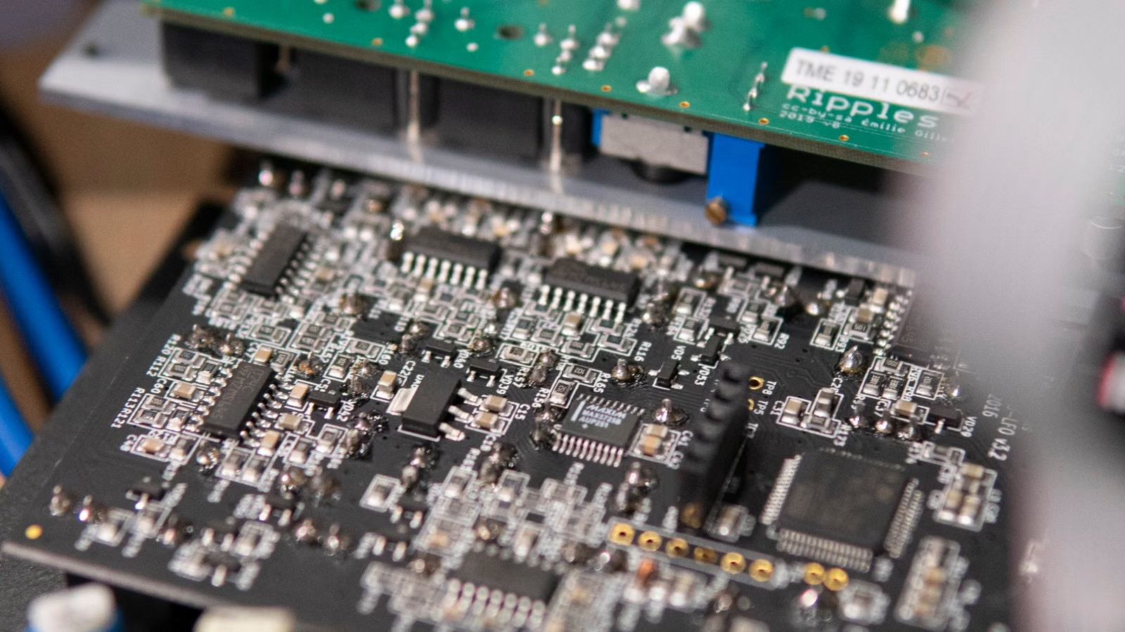
The HBM packaging bottleneck lies in whether multiple layers of memory dies can be stacked reliably and connected to AI compute chips at extremely high speed. You should not think of HBM as simply a faster memory module. It is closer to a three-dimensional memory system: multiple DRAM dies are vertically connected through TSVs, stacked through TCB or similar bonding processes, and then integrated with GPUs or AI ASICs inside a 2.5D advanced package. If any one step suffers from low yield, final AI accelerator shipments can slow down.
Conventional DRAM is more of a planar product. HBM is a 3D stack. Each DRAM layer must be thinned, aligned, connected, and tested. The more layers there are, the greater the yield pressure. By the HBM3E and HBM4 generations, bandwidth, capacity, I/O count, and thermal pressure per HBM stack all rise sharply. As a result, packaging is no longer just a back-end manufacturing step. It becomes a critical factor that determines system-level performance.
You can break the HBM bottleneck into four broad categories: memory die capacity, TSV and stacking processes, TCB or hybrid bonding equipment, and CoWoS, substrates, testing, and system-level packaging capacity. If any one of these areas is constrained, the market sees the same end result: tight AI chip supply.
| Segment | Role | Main Bottleneck | Related Company Types |
|---|---|---|---|
| DRAM wafers | Provide HBM memory dies | Advanced DRAM capacity and yield | SK hynix, Samsung, Micron |
| TSV and thinning | Enable vertical interconnects | Wafer handling precision and mechanical strength | Memory makers, back-end equipment suppliers |
| TCB bonding | Stack multiple DRAM dies | Alignment, temperature, and warpage control | Hanmi, ASMPT, BESI, and others |
| CoWoS / 2.5D packaging | Connect GPUs and HBM | Interposers, substrates, and packaging slots | TSMC, ASE, Amkor, and others |
| Testing and metrology | Control shipment quality | Defect inspection, electrical testing, failure analysis | KLA, Advantest, Teradyne, and others |
The most easily overlooked factor is the “yield multiplication effect.” If an HBM stack contains 8, 12, or even 16 DRAM layers, a defect in any single layer can affect the entire stack. The higher the layer count, the more final yield depends on material consistency, thermal process windows, die warpage, micro-bump quality, and test screening. In other words, HBM expansion is not just about adding capacity. It is a competition in high-precision manufacturing and high-density packaging.
Summary: The essence of the HBM packaging bottleneck is that high-bandwidth memory has evolved from a single chip into a complex three-dimensional system. When you evaluate the HBM supply chain, you cannot focus only on memory maker capacity. You also need to look at TSVs, TCB, hybrid bonding, CoWoS, substrates, and testing capability. What often limits AI chip shipments is not whether a single chip design has been completed, but whether multiple chips can be integrated reliably under high yield, high bandwidth, and controlled thermal conditions. For investors, this means the HBM theme should be analyzed not only as a memory pricing cycle, but as a broader advanced packaging systems capability.
Why Has CoWoS Become the Core Bottleneck in AI Chip Delivery?

CoWoS has become a core bottleneck because high-end AI GPUs and ASICs need to place compute dies and HBM inside the same high-density package to achieve sufficient bandwidth and lower latency. TSMC’s CoWoS-S targets AI and high-performance computing by connecting logic chips and HBM cubes through a silicon interposer. If there are not enough CoWoS slots, final AI accelerators may still be delayed even when GPU dies and HBM are already available.
One of the key bottlenecks in AI training and inference is memory bandwidth. Model parameters, activations, and intermediate computation results need to move rapidly between the GPU and HBM. Traditional PCB connections are too long, offer insufficient bandwidth density, and consume more power. Advanced packaging brings compute chips and HBM as close together as possible. That is where CoWoS creates value: it turns multiple large dies, HBM stacks, and interposers into one high-performance packaging system.
At its 2026 North America Technology Symposium, TSMC said it was producing 5.5-reticle-size CoWoS and planned to mass-produce 14-reticle-size CoWoS in 2028, capable of integrating around 10 large compute dies and 20 HBM stacks. This shows the direction of CoWoS scaling clearly: AI chips require larger package areas, more HBM, higher interconnect density, and stronger thermal handling.
But CoWoS shortages cannot be solved by TSMC capacity expansion alone. TrendForce noted that severe shortages in global 2.5D packaging capacity are expected to start easing only slightly in 2027. The bottleneck also involves outsourced OSAT demand, substrates, materials, equipment, and testing capacity. Even if the supply-demand gap narrows, a narrowing CoWoS supply gap does not mean high-end AI packaging becomes fully relaxed, because each new generation of chips tends to consume larger package areas and more complex packaging resources.
| CoWoS Type | Main Structure | Best-Fit Use Case | Key Bottleneck |
|---|---|---|---|
| CoWoS-S | Large silicon interposer | High-end AI GPUs and HPC | High cost, large area, tight capacity |
| CoWoS-L | Local silicon interconnect + RDL | Larger packages and more flexible integration | Design complexity and yield ramp |
| CoWoS-R | RDL interposer | Balance of cost and flexibility | Signal integrity and material control |
You can think of CoWoS as the “delivery platform” for AI chips. Advanced nodes determine compute die performance. HBM determines memory bandwidth. CoWoS determines whether the two can actually become a sellable, deployable, and stable AI accelerator. The more demanding the workload—large-model training, high-end inference, or custom ASICs—the more dependent it becomes on this high-density packaging platform.
Summary: CoWoS matters because it connects GPUs or ASICs and HBM into a complete AI computing system. If CoWoS capacity, substrates, materials, or testing capability is insufficient, AI chip delivery will be affected. When evaluating CoWoS-related opportunities, you should focus on larger package sizes, higher HBM stack counts, customer capacity reservations, OSAT division of labor, and upstream equipment delivery. It is not enough to see whether a company is labeled an “advanced packaging concept.” CoWoS is one of the closest supply-chain links to the actual delivery bottleneck in AI hardware.
What Problems Do TCB and Hybrid Bonding Solve?
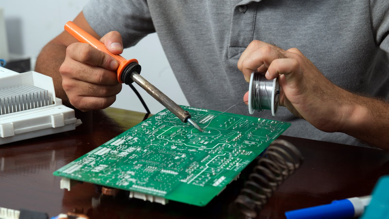
TCB solves the current problem of reliably stacking multiple HBM dies, while hybrid bonding addresses the next stage of higher-density, lower-power, finer-pitch interconnects. You can think of TCB as the main process used in today’s HBM mass production, while hybrid bonding is an important upgrade path for HBM4, HBM4E, and later generations. The two are not a simple replacement relationship. They are more like parallel routes: one offers near-term production certainty, the other offers long-term technology upside.
TCB stands for thermo-compression bonding. It uses temperature, pressure, and precise alignment to form stable connections between die and die, or between die and substrate. In HBM stacking, TCB has to manage micro-bumps, thermal process windows, pressure uniformity, and warpage control. The more layers there are, and the thinner the dies become, the more sensitive the package becomes to thermal stress and mechanical deformation. That makes TCB equipment precision and throughput extremely important.
TrendForce reported that SK hynix placed an order for 44.2 billion won TCB bonders from Hanmi Semiconductor for HBM4-related capacity ramp-up. Orders like this show that HBM expansion is not only about buying more front-end tools. Back-end stacking and bonding equipment can also become a major area of capital expenditure.
Hybrid bonding follows a different logic. It emphasizes Cu-to-Cu direct bonding and reduces the pitch and resistance limitations associated with traditional micro-bumps. When Samsung showcased HBM4E at GTC 2026, it noted that hybrid copper bonding could support HBM with more than 16 layers and reduce thermal resistance by more than 20% compared with TCB. For higher-layer-count and higher-bandwidth HBM, lower thermal resistance and higher interconnect density both matter.
| Dimension | TCB | Hybrid Bonding |
|---|---|---|
| Technology maturity | More mature today, with more mass production experience | Still being introduced, with yield ramp as the key issue |
| Interconnect method | Micro-bumps + thermo-compression | Cu-to-Cu direct bonding |
| Main advantage | Mature supply chain and more direct order conversion | Higher density, shorter interconnects, lower power |
| Main challenge | Warpage, thermal damage, throughput control | Surface cleanliness, flatness, equipment cost |
| Investment implication | Higher short-term equipment order visibility | Greater long-term technology positioning |
There are two common mistakes to avoid when evaluating TCB and hybrid bonding. The first is assuming that hybrid bonding will immediately replace TCB across the board. Advanced packaging process adoption requires customer qualification, equipment tuning, material alignment, and yield validation. It will not switch overnight. The second mistake is focusing only on technical superiority while ignoring production timing. Whether an equipment company benefits still depends on whether customers place orders, whether delivery runs smoothly, and whether revenue appears in financial results.
Summary: TCB is a key process for current HBM mass production, while hybrid bonding is an important direction for next-generation high-density packaging. TCB-related equipment orders are more likely to appear in near-term revenue, while hybrid bonding functions more like a long-term technology option for the HBM4, HBM4E, and HBM5 eras. When analyzing related companies, you should look at technology roadmaps, customer qualification, equipment delivery, yield, and mass production schedules at the same time. A more advanced technology does not automatically mean faster near-term revenue. Production maturity, customer adoption timing, and equipment share are the real investment variables.
Why Can Equipment Suppliers Benefit, and Why Does Relevance Not Equal Earnings Leverage?
Equipment suppliers can benefit because HBM and CoWoS expansion requires more TCB tools, die bonders, hybrid bonding systems, inspection tools, metrology tools, and test equipment. But relevance does not equal earnings leverage. Even if a company is technically involved in advanced packaging, it may not have core customer share, repeat orders, high margins, or enough revenue exposure. When evaluating equipment suppliers, you need to move from “is it related?” to “is it inside the mass production supply chain?”
ASMPT’s orders help illustrate this point. In December 2025, the company announced additional orders for 15 C2S TCB tools for advanced AI computing chips. It had earlier announced orders for nineteen C2S TCB tools and said its C2S TCB solution was part of the customer’s Process of Record. For equipment companies, POR status, repeat orders, and major customer validation carry far more weight than simply mentioning advanced packaging in a product description.
BESI is a clearer observation window for hybrid bonding. BESI reported Q1-26 orders of €269.7 million, up 104.5% year over year. Reuters also noted that BESI hybrid bonding demand was an important driver of order growth. Hybrid bonding is more closely linked to HBM4, chiplets, and 3D integration, but the revenue cycle still depends on how quickly customers move into mass production.
You can screen equipment supplier relevance using the following criteria:
| Evaluation Factor | What to Watch | Common Mistake |
|---|---|---|
| Customer qualification | Whether the company is in leading customers’ mass production flow | Looking only at technical marketing |
| Order quality | Whether there are follow-on orders and repeat purchases | Treating a prototype order as mass production |
| Product exposure | Whether advanced packaging revenue share is rising | Ignoring drag from legacy businesses |
| Delivery timing | Whether equipment delivery matches customer expansion | Looking at orders without revenue timing |
| Margin leverage | Gross margin, service revenue, and product mix | Watching revenue but ignoring profit |
| Valuation risk | Whether growth is already priced in | Linearly extrapolating industry momentum |
When supply-chain opportunities move into actual trading, cost structure also matters. Popular semiconductor stocks, ADRs, Hong Kong-listed names, and ETFs can be volatile, and frequent rebalancing can amplify trading costs. Biya charges 0 USD commission for U.S. stock trading, while platform fees, external institution fees, and other charges are subject to U.S. stock trading fees and order-page disclosures. The above information explains public market information, trading rules, and fee structures only. It does not constitute investment advice. Service availability depends on the user’s location, identity verification result, platform rules, and applicable laws and regulations.
Summary: Equipment suppliers are one of the most direct ways to observe the HBM packaging bottleneck, but “being related” should not be treated as “high earnings leverage.” The real indicators to track are customer qualification, repeat orders, equipment share, advanced packaging revenue exposure, gross margin, and delivery cycles. TCB equipment suppliers may have clearer short-term order visibility. Hybrid bonding equipment suppliers may have greater long-term technology upside. Test and metrology suppliers may benefit from rising yield requirements. Investors should also factor in trading costs, volatility risk, and valuation digestion when building an investment framework.
From HBM3E to HBM4, Will the Bottleneck Ease or Intensify?
HBM4 will not necessarily ease packaging bottlenecks. It may actually intensify them. The reason is straightforward: HBM4 increases interface width, bandwidth, capacity, and layer count. AI chips can gain stronger memory bandwidth, but the packaging side must deal with more complex signal integrity, thermal management, die warpage, test coverage, and CoWoS integration. The stronger the performance, the harder the packaging challenge.
JEDEC released the JESD270-4 HBM4 standard in 2025. As the generation after HBM3, HBM4 emphasizes higher bandwidth, energy efficiency, and capacity. Wider I/O, higher pin speed, and more channels can improve AI training and inference efficiency, but they also require higher interconnect density and tighter electrical requirements in packaging design.
Micron has disclosed HBM4 36GB 12H for NVIDIA Vera Rubin, with bandwidth of more than 2.8TB/s per stack and improved power efficiency versus the previous generation. Samsung’s HBM4E showcase pushed targets toward higher pin speed and higher bandwidth, while emphasizing the importance of hybrid copper bonding for stacks above 16 layers and for thermal resistance improvement. The competition among memory makers is no longer only about “larger capacity.” It is increasingly about packaging, base dies, thermal management, and customer platform co-design.
| Generation | Main Improvement | Packaging Pressure | Supply-Chain Watchpoint |
|---|---|---|---|
| HBM3E | Higher bandwidth and capacity | TCB, thermal management, yield | Memory maker expansion, CoWoS allocation |
| HBM4 | Wider interface and higher bandwidth | Base die, stacking, testing | Parallel use of TCB and hybrid bonding |
| HBM4E | Higher speed and capacity | Thermal resistance, fine pitch, materials | Hybrid bonding, inspection, packaging materials |
| HBM5 | Higher system integration | 3D packaging, power, cost | Equipment, materials, design collaboration |
The bottleneck will also shift. Earlier, the market focused more on “who can supply HBM.” Going forward, it will increasingly focus on “who can integrate HBM reliably.” As HBM moves into HBM4 and HBM4E, base logic dies, custom base dies, CoWoS slots, C2S bonding, die-to-wafer bonding, thermal interface materials, and system-level testing all become more important. This is why advanced packaging equipment, materials, and testing companies keep appearing in the AI hardware investment narrative.
Summary: HBM4 raises the performance ceiling for AI chips, but it does not automatically remove packaging bottlenecks. Higher bandwidth, larger capacity, and more layers increase the difficulty of bonding, thermal management, testing, and system integration. When evaluating HBM4 supply-chain opportunities, you should not focus only on whether memory makers announce mass production. You also need to assess customer platform adoption, packaging route maturity, CoWoS capacity matching, and whether hybrid bonding has reached stable yield. The bottleneck may shift from “whether HBM is available” to “whether HBM can be integrated at high yield and large scale.”
How Can Investors Evaluate the Real Link Between CoWoS, TCB, and Equipment Suppliers?
The most effective way to evaluate real relevance is to use a four-layer framework: whether the bottleneck actually exists, whether the company sits in a hard-to-replace position, whether orders can enter financial statements, and whether valuation has already priced in the growth. AI hardware momentum will produce many concept-driven narratives, but only companies involved in critical capacity, critical processes, critical equipment, and major customer qualification are more likely to translate industry demand into financial results.
The first layer is whether the bottleneck is real. Reuters reported that Broadcom referred to TSMC capacity as a bottleneck and noted that AI demand had placed pressure on advanced nodes, adjacent supply-chain links, and certain components. This kind of information shows that AI chip delivery constraints are not just an HBM issue. They involve front-end manufacturing, packaging, PCBs, optical modules, materials, and equipment at the same time.
The second layer is where the company sits in the chain. Packaging platforms such as TSMC, ASE, and Amkor are closer to CoWoS slots. HBM makers such as SK hynix, Samsung, and Micron are closer to memory stacking. Equipment suppliers such as Hanmi, ASMPT, BESI, and Applied Materials are closer to bonding and advanced packaging tools. Test and metrology companies are tied to yield control. Different positions mean different business models, order cycles, and valuation logic.
The third layer is the path to financial conversion. You need to monitor backlog, capex, customer concentration, delivery cycles, advanced packaging revenue exposure, gross margin, service revenue, and inventory changes. If a company’s advanced packaging business is still a small portion of revenue, then even strong technical relevance may not create much near-term profit leverage. By contrast, if a company enters a leading customer’s mass production flow and receives repeat orders, relevance is more likely to turn into financial performance.
| Evaluation Dimension | What to Look At | Mistake to Avoid |
|---|---|---|
| Technical relevance | Participation in HBM, CoWoS, TCB, or hybrid bonding | Relying only on concept labels |
| Customer qualification | Entry into leading customers’ supply chains | Ignoring qualification cycles |
| Order conversion | Repeat orders and revenue recognition | Treating rumors as earnings |
| Profit leverage | Gross margin, revenue exposure, scale effects | Looking only at order size |
| Valuation risk | Whether growth is already priced in | Linearly extrapolating industry momentum |
If you want to track related stocks, ADRs, Hong Kong-listed companies, or ETFs, you can use Biya to follow U.S. stocks, Hong Kong stocks, and digital asset market information, and build a watchlist through U.S. stock information search. A more disciplined approach is to first group companies into HBM makers, CoWoS platforms, bonding equipment suppliers, test and metrology companies, and materials or substrate suppliers, then review financial reports and order announcements one by one. Putting all advanced packaging companies into one basket can easily blur the differences in revenue exposure and risk.
Summary: The investment value of CoWoS, TCB, and equipment suppliers comes from the combination of real bottlenecks, critical supply-chain positions, customer qualification, order conversion, and reasonable valuation. You should not assume that a company will benefit simply because it appears somewhere in the advanced packaging chain. You also should not ignore equipment delivery cycles, customer concentration, and valuation risk just because HBM demand is strong. A better analytical path is to identify where the bottleneck is, determine who can solve that bottleneck, and then evaluate whether solving it can show up in revenue, profit, and cash flow.
If you continue to follow HBM, CoWoS, AI chips, and semiconductor equipment stocks, the next step is not to chase every market rumor. It is to build a repeatable tracking framework: where the company sits in the supply chain, who its customers are, when orders are recognized, whether gross margin is improving, and whether valuation has already reflected expectations. Biya supports U.S. stock and Hong Kong stock trading as well as multi-asset market viewing. You can use the Biya App to follow related companies, industry ETFs, earnings dates, and price movements. U.S. stock trading commission is 0 USD, while platform fees, external institution fees, and other charges are subject to the fee center and order-page disclosures. The above information is for understanding public market information and supply-chain logic only. It does not constitute investment advice. Before trading, you should consider your own risk tolerance, applicable rules in your location, and the platform’s actual service availability.
FAQ
What Is the Difference Between an HBM Packaging Bottleneck and HBM Capacity Shortage?
An HBM capacity shortage mainly refers to insufficient output of memory dies and HBM stacks. An HBM packaging bottleneck also includes CoWoS, TCB, substrates, materials, testing, and yield. The two are related, but they are not the same issue. Even if memory makers expand HBM capacity, limited advanced packaging slots or bonding equipment can still constrain AI chip delivery.
Why Does a CoWoS Shortage Affect AI GPU Shipments?
A CoWoS shortage affects AI GPU shipments because high-end AI GPUs usually need CoWoS to integrate compute dies and HBM in the same package. Having GPU dies and HBM available separately does not mean the final product is ready to ship. Packaging, substrates, testing, and yield must also meet mass production requirements.
How Are TCB Equipment Suppliers Related to the HBM Investment Theme?
TCB equipment suppliers are related to the HBM investment theme because TCB is a key equipment step in HBM die stacking and advanced packaging. As HBM layer counts increase, bonding precision, temperature control, and throughput requirements rise. Investment analysis should still focus on customer qualification, order size, delivery timing, and revenue exposure.
Will Hybrid Bonding Quickly Replace TCB?
Hybrid bonding is unlikely to fully replace TCB in the short term. It is more likely to be introduced in parallel with TCB. Hybrid bonding is well suited for higher-density, lower-power, finer-pitch next-generation packaging, but mass production requires surface cleanliness, flatness, equipment coordination, and yield validation. TCB still has a mature production base.
How Can Individual Investors Evaluate CoWoS-Related Companies?
Individual investors should evaluate CoWoS-related companies by first determining whether the company is in a core bottleneck segment, then reviewing customer qualification, order conversion, advanced packaging revenue exposure, and margin trends. Technical relevance alone is not enough. The financial conversion path must be clear, and investors should be cautious if valuation has already priced in much of the expected growth.
Will HBM4 Mass Production Ease Packaging Bottlenecks?
HBM4 mass production will not necessarily ease packaging bottlenecks. Some bottlenecks may intensify. HBM4 increases bandwidth, interface width, and capacity, but it also raises the difficulty of stacking, bonding, thermal management, testing, and CoWoS integration. The key is not only whether HBM4 can be produced, but whether it can be integrated into AI chip systems at high yield and large scale.
*This article is provided for general information purposes and does not constitute legal, tax or other professional advice from BiyaPay or its subsidiaries and its affiliates, and it is not intended as a substitute for obtaining advice from a financial advisor or any other professional.
We make no representations, warranties or warranties, express or implied, as to the accuracy, completeness or timeliness of the contents of this publication.
Related Blogs of

Why Is Seagate Getting Attention from AI Data Centers? Can a Non-Chip Stock Benefit Too?


How to Analyze Micron’s HBM Business Share When Exact Data Is Unavailable


How to Read Seagate STX Earnings: Nearline HDD, Free Cash Flow, and Shareholder Returns


HPE, Dell, and Enterprise Storage: Which Company Looks More Like an AI Infrastructure Player?
Choose Country or Region to Read Local Blog
 Australia
 Austria
 Belgium
 Canada
 Cyprus
 Czech Republic
 Denmark
 Estonia
 Finland
 France
 Germany
 Greece
 Hong Kong
 India
India Indonesia
 Ireland
 Italy
Italy Japan
Japan Latvia
 Lithuania
 Luxembourg
 Malaysia
 Malta
Malta Morocco
 Nepal
Nepal Netherlands
 New Zealand
 Norway
 Pakistan
 Philippines
 Poland
 Portugal
 Romania
 Singapore
 Slovakia
 Slovenia
 South Africa
 South Korea
 Spain
Spain Sweden
 Thailand
 The United States
 Turkey
 United Arab Emirates
 United Kingdom
 Vietnam
Contact Us




BIYA GLOBAL LLC is registered with the Financial Crimes Enforcement Network (FinCEN), an agency under the U.S. Department of the Treasury, as a Money Services Business (MSB), with registration number 31000218637349, and regulated by the Financial Crimes Enforcement Network (FinCEN).
BIYA GLOBAL LIMITED is a registered Financial Service Provider (FSP) in New Zealand, with registration number FSP1007221, and is also a registered member of the Financial Services Complaints Limited (FSCL), an independent dispute resolution scheme in New Zealand.