What Is HBM? Why AI Chips Depend on High Bandwidth Memory


HBM stands for High Bandwidth Memory. It is a high-speed memory solution that vertically stacks multiple layers of DRAM and places them close to GPUs or AI accelerators through advanced packaging. AI chips depend on HBM not simply because it is “more expensive memory,” but because large-model training and inference require massive amounts of parameters, activations, gradients, and KV Cache to move within extremely short time windows. Ordinary DDR or GDDR is often unable to meet bandwidth, power, packaging distance, and system efficiency requirements at the same time, making HBM one of the core bottlenecks for high-end AI chips.
Key Takeaways
- HBM is high bandwidth memory created by vertically stacking multiple DRAM layers.
- AI chips need HBM because large-scale data movement creates extreme pressure.
- HBM is not hard drive storage, and it is different from ordinary DDR and GDDR.
- HBM3E and HBM4 are pushing AI chip performance to the next stage.
- The HBM supply chain involves memory makers, packaging, GPUs, equipment, and materials.
- HBM is a high-growth theme, but it also carries capacity, cost, valuation, and cycle risks.
What Is HBM? A Simple Explanation of High Bandwidth Memory
HBM, or High Bandwidth Memory, is a memory solution that vertically stacks multiple DRAM chips and places them close to GPUs or AI accelerators through advanced packaging technologies such as TSVs, micro-bumps, and silicon interposers. It is not a hard drive, nor is it just a simple upgrade of ordinary graphics memory. It is a high-bandwidth, low-power, highly integrated memory technology designed for AI training, AI inference, high-performance computing, and graphics workloads.
You can think of HBM as “high-speed working memory placed extremely close to the computing chip.” It solves the problem of fast data reading and writing near the processor, rather than long-term file storage. SSDs, NAND Flash, and hard drives are used for persistent storage. HBM belongs to the DRAM family, meaning data is not retained after power loss. Its job is to read and write data at very high speed during computation.
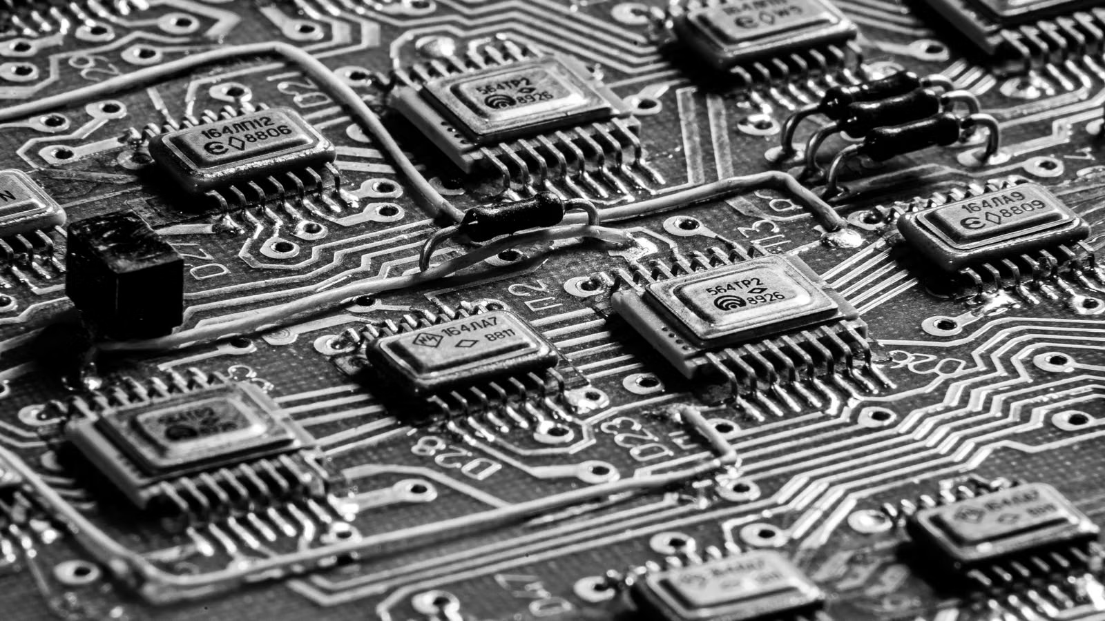
Industry discussions of High Bandwidth Memory usually describe it as 3D-stacked DRAM. Multiple DRAM dies are stacked vertically like floors in a building, then connected through TSVs, which act as vertical channels. Compared with placing memory chips flat around a graphics card or motherboard, HBM can deliver wider data channels within a smaller package area. Synopsys also describes 3D-stacked SDRAM as a high-speed memory interface serving vertically stacked synchronous DRAM.
The key to HBM is not just frequency, but the “very wide interface.” Ordinary memory often relies more heavily on increasing frequency, while HBM improves total bandwidth by widening the data path. Cadence’s description of HBM3 PHY notes that HBM3 can use a 1024-bit total data width and is designed for 2.5D systems and silicon interposer routing. This also explains why HBM must be understood together with advanced packaging.
| Type | Main Use | Volatile? | Location | Relationship with AI Chips |
|---|---|---|---|---|
| HBM | High-speed memory for AI GPUs, HPC, and AI accelerators | Yes | Close to GPU/ASIC, in-package or near-package | Directly affects bandwidth, capacity, and energy efficiency |
| DDR | CPU system memory | Yes | DIMM slots or server memory channels | Can serve as system memory, but farther from the accelerator |
| GDDR | Graphics memory and GPU workloads | Yes | On PCB around the GPU | Suitable for graphics cards and some inference cards |
| SRAM/Cache | On-chip high-speed cache | Yes | Inside the chip | Very low latency but small capacity and high cost |
| NAND Flash/SSD | Long-term data storage | No | SSDs and storage devices | Does not serve as core training memory |
Summary: HBM is high-speed memory placed next to AI chips. It is not a hard drive, SSD, or ordinary storage device. Through vertically stacked DRAM, TSV interconnects, ultra-wide interfaces, and advanced packaging, HBM brings high bandwidth memory as close as possible to GPUs or AI accelerators. It solves the problem of “the chip can calculate very fast, but data cannot be fed fast enough.” To understand HBM, you should not only look at capacity, but also bandwidth, power consumption, packaging distance, yield, and system design, because all these factors determine the real efficiency of AI chips.
Why Do AI Chips Depend on HBM? The Real Bottleneck Is Data Movement
AI chips depend on HBM because large-model training and inference are often limited not only by compute power, but also by memory bandwidth, capacity, and power consumption. The Tensor Cores or matrix compute units inside GPUs can execute massive parallel operations, but model parameters, activations, gradients, and KV Cache must be continuously read from memory. If memory bandwidth cannot keep up, the AI chip has to wait for data, causing real utilization to drop significantly.
The data pressure during large-model training is the most obvious. When training a large model, the chip must repeatedly read model parameters, store activations, calculate gradients, and update optimizer states. The larger the parameter count, the more frequent the data movement. The larger the batch size, the higher the requirements for memory capacity and bandwidth. Multi-GPU training also has to handle both internal memory access within each card and interconnect communication between chips. In its discussion of the Hopper architecture, NVIDIA describes the HBM3 memory subsystem as one of H100’s key capabilities and highlights its major improvement in memory bandwidth compared with the previous generation.
Inference is also becoming increasingly dependent on HBM. Many people assume inference means “running the model once,” but large language models generate output token by token. Each generated token requires access to model weights and context cache. Longer context windows significantly increase KV Cache usage; high-concurrency inference means multiple user requests occupy memory at the same time; multimodal models add additional intermediate data from images, audio, video, and other inputs. When HBM capacity is insufficient, systems may have to move part of the data to slower memory or storage, increasing both latency and cost.
You can break AI chip performance into four parts:
- Whether the compute units are powerful enough.
- Whether HBM bandwidth can continuously feed data.
- Whether HBM capacity can hold the model and cache.
- Whether chip interconnects, software, and scheduling work together.
NVIDIA’s H100 offers 80GB or 94GB of GPU memory depending on the version, with memory bandwidth of up to 3.35TB/s or 3.9TB/s. The H200 raises HBM3e capacity to 141GB and bandwidth to 4.8TB/s. This upgrade shows that high-end AI GPU competition is no longer just about Tensor Core compute. It is increasingly also about HBM capacity and bandwidth.
| AI Workload | Why It Needs HBM | Main Pressure |
|---|---|---|
| Large-model pretraining | Frequent reading and writing of parameters, activations, and gradients | Bandwidth, capacity, power |
| Large-model fine-tuning | Training states must be saved | Capacity, memory efficiency |
| High-concurrency inference | Multiple requests occupy memory at once | Bandwidth, KV Cache |
| Long-context inference | Longer context means larger cache | Capacity, latency |
| Multimodal models | Image, audio, and video data are more complex | Bandwidth, scheduling |
| Scientific computing/HPC | Large matrices and large-scale data flows | Bandwidth, energy efficiency |
Summary: AI chips depend on HBM because large-model computing is heavily constrained by data movement. Peak compute power is only a theoretical upper limit. Real throughput depends on whether data can be delivered to compute units continuously, with low latency and low power consumption. HBM provides higher bandwidth, shorter packaging distance, and better energy efficiency, allowing GPUs or AI ASICs to spend less time waiting for data. Without HBM, high-end AI chips may have strong theoretical compute power, but training throughput, inference latency, and system efficiency would be limited by the memory wall.
How Is HBM Different from DDR and GDDR? Why They Cannot Simply Replace One Another
HBM, DDR, and GDDR are all memory technologies, but they serve different roles. DDR is mainly used as CPU system memory, with large capacity and relatively low cost. GDDR is commonly used in graphics cards, offering higher bandwidth and fitting consumer GPUs well. HBM, however, uses vertical stacking and an ultra-wide interface to deliver higher bandwidth, lower energy per bit transferred, and shorter packaging distance. AI chips choose HBM because it is better suited for dense computing and high-bandwidth data exchange, not because DDR or GDDR is useless.
DDR’s strengths are maturity, low cost, and flexible capacity expansion. Servers can install many DDR memory modules to support CPU workloads, databases, virtualization, and general computing. But DDR is usually not placed in the same advanced package as an AI accelerator. It is farther away and has narrower channels, so it cannot directly serve dense matrix computing in high-end GPUs the way HBM can. In AI systems, DDR is more like system-level memory support, rather than core high-speed accelerator memory.
GDDR is closer to graphics memory and is widely used in gaming GPUs, professional graphics cards, and some inference cards. It offers higher bandwidth than DDR, while its cost and manufacturing maturity are better than HBM. That makes it valuable in consumer GPUs and mid-to-low-end AI inference devices. But GDDR usually requires more chips placed around the GPU, and PCB area, signal integrity, and power consumption can become constraints. When high-end AI training cards require higher memory density and better bandwidth per watt, HBM becomes much more attractive.
HBM’s core advantage is optimizing bandwidth, power consumption, and packaging distance as one system. AMD’s Instinct MI300 Series emphasizes large memory density, high bandwidth, and suitability for AI and HPC workloads, showing that high-end AI accelerators now treat the memory system as part of their core product competitiveness. HBM’s weaknesses are also clear: high cost, complex packaging, strict yield requirements, and tight supply chains. It is not suitable for every device.
| Dimension | HBM | GDDR | DDR | Impact on AI Chips |
|---|---|---|---|---|
| Bandwidth | Highest, suitable for high-end AI | High, suitable for GPUs | Relatively lower | HBM better supports matrix computing |
| Capacity expansion | Stack capacity is improving, but cost is high | Medium | Flexible and lower cost | DDR is better for system memory |
| Power consumption | Lower energy per bit transferred | Higher | Manageable | HBM better fits data center efficiency needs |
| Packaging | 2.5D/3D packaging, close to GPU | Around GPU on PCB | Motherboard memory channel | HBM is closer and offers higher bandwidth |
| Cost | High | Medium | Low | HBM is not suitable for low-cost devices |
| Typical use | AI GPUs, HPC, AI ASICs | Graphics cards, inference cards | CPU servers, PCs | Different roles, not full replacements |
Summary: HBM does not replace DDR or GDDR across all scenarios. Instead, it is better suited for solving bandwidth and energy efficiency problems in high-end AI chip systems. DDR works well as general-purpose system memory. GDDR remains suitable for consumer GPUs and some inference cards. HBM serves high-end AI training, inference, and HPC. To understand the difference, do not only compare capacity. You also need to consider packaging distance, bandwidth per watt, system design, and cost. AI chips use HBM because, at very high compute density, the memory system must be as close as possible to the compute units.
How Has HBM Evolved from HBM2 to HBM4? Why AI Chips Keep Chasing Upgrades
HBM has evolved toward higher bandwidth, larger capacity, lower power consumption, and more complex packaging. From HBM2 and HBM2E to HBM3, HBM3E, and now HBM4, per-stack bandwidth, stack height, and interface capabilities continue to improve. AI chips keep chasing HBM upgrades because model size, context length, inference concurrency, and multimodal computing are all increasing. Older generations of memory can quickly become system bottlenecks.
HBM2 and HBM2E laid the foundation for high-performance computing and early AI acceleration. They solved the bandwidth limits of traditional graphics memory and allowed GPUs, FPGAs, and HPC accelerators to obtain higher memory bandwidth within a smaller package area. But as generative AI took off, large-model parameter counts expanded rapidly. Training and inference began demanding more capacity, bandwidth, and energy efficiency, making HBM2E less sufficient for top-tier AI training platforms.
HBM3 and HBM3E became the main focus after the rise of generative AI. The evolution of platforms such as NVIDIA H100 and H200 shows that AI chip makers increasingly treat HBM capacity and bandwidth as product differentiators. SK hynix has announced volume production of 12-layer HBM3E, Samsung has developed 36GB HBM3E 12H, and Micron’s HBM3E highlights an 8-high, 24GB cube with bandwidth above 1.2TB/s.
HBM4 pushes the competition into the next stage. The JEDEC-related JESD270-4 HBM4 Standard points toward higher data processing speeds, while Micron has disclosed HBM4 36GB 12H designed for NVIDIA Vera Rubin, emphasizing bandwidth above 2.8TB/s and higher energy efficiency. HBM4 is not just an upgrade for memory makers. It also affects GPU controllers, packaging substrates, silicon interposers, testing, and cooling systems.
| Generation | Main Features | Meaning for AI Chips | Main Risks |
|---|---|---|---|
| HBM2 | Mature high-bandwidth stacked memory | Supports early HPC and GPU acceleration | Capacity and bandwidth gradually become insufficient |
| HBM2E | Higher capacity and bandwidth | Suitable for early AI acceleration upgrades | Hard to support larger models |
| HBM3 | Major bandwidth improvement | Becomes a key selling point of high-end AI GPUs | Tight supply and high cost |
| HBM3E | Higher capacity and bandwidth | Supports long-context and high-concurrency inference | High customer qualification and yield requirements |
| HBM4 | Higher interface capability and system integration | Designed for next-generation AI platforms | More complex packaging, cooling, and cost |
Summary: HBM upgrades are not just a parameter race. They are driven by AI system demand. The larger the model, the longer the context, and the higher the inference concurrency, the more AI chips need larger capacity and higher bandwidth. HBM3E allows high-end AI GPUs to handle larger models and heavier inference workloads. HBM4 pushes bandwidth, capacity, and packaging complexity even higher. Future HBM competition will extend beyond memory chips themselves into the combined capabilities of memory makers, GPU vendors, foundries, advanced packaging suppliers, equipment and materials companies, and system builders.
Who Is Involved in the HBM Supply Chain? It Is Not Just SK hynix, Samsung, and Micron
The HBM supply chain is not just about the three major memory makers. SK hynix, Samsung Electronics, and Micron produce HBM stacks, but for HBM to enter AI chips, GPU and ASIC designers, wafer foundries, advanced packaging providers, packaging equipment companies, testing companies, materials suppliers, and server manufacturers must all work together. When tracking the HBM theme, the key question is not only “who produces HBM,” but also “who integrates HBM into AI systems.”
The upstream layer includes memory makers, materials, and equipment. Memory makers are responsible for DRAM dies, stacking, TSVs, product validation, and customer qualification. HBM is more complex than ordinary DRAM because it requires thinner DRAM dies, higher stacking, stricter thermal management, and higher yield. When supply is tight, leading AI chip customers are more likely to secure capacity, which is why long-term agreements, prepayments, and qualification barriers often appear in the HBM industry.
The midstream layer includes wafer foundries and advanced packaging. HBM is not a memory module inserted into a motherboard. It must be integrated with GPUs, AI ASICs, or accelerator chips. TSMC’s CoWoS explains that silicon interposers can accommodate logic chiplets and allow HBM cubes to be stacked on top. TSMC 3DFabric also places SoIC, CoWoS, and InFO under the broader demand for high performance, high energy efficiency, low latency, and high integration. This means HBM bottlenecks often appear not only at memory makers, but also in advanced packaging capacity, silicon interposers, substrates, equipment, and testing.
The downstream layer includes AI chip vendors, cloud companies, and server makers. NVIDIA, AMD, Broadcom, Marvell, and custom ASIC developers determine HBM platform specifications. Cloud providers and model companies drive demand for training clusters, inference clusters, and data center capital expenditure. Server OEMs/ODMs, power systems, and cooling systems determine whether those chips can be deployed at scale. HBM demand is not unlimited. It is still constrained by budgets, power, cooling, compute utilization, and the commercialization pace of AI applications.
| Segment | Representative Participants | Main Role | Investment Metrics to Watch |
|---|---|---|---|
| Memory makers | SK hynix, Samsung, Micron | Produce HBM stacks | Capacity, yield, customer qualification |
| Wafer foundries | TSMC and others | Produce GPU/ASIC logic chips | Advanced nodes, AI orders |
| Advanced packaging | TSMC, OSATs, packaging companies | Integrate logic chips and HBM | CoWoS/2.5D capacity |
| Equipment and materials | Packaging equipment, substrates, silicon interposer materials | Support mass production and yield | Orders, delivery, material supply |
| GPU/ASIC vendors | NVIDIA, AMD, custom chip makers | Design AI accelerators | Platform upgrades, shipment schedule |
| Cloud and server companies | Hyperscalers, OEMs/ODMs | Absorb AI chip demand | CAPEX, rack delivery, utilization |
Summary: HBM is a cross-company, cross-process, cross-system supply chain, not a single memory product. The real factors shaping HBM supply and demand include memory maker capacity, advanced packaging capacity, AI chip design, cloud capital expenditure, server deployment pace, and power and cooling conditions. To analyze the HBM theme, do not only watch SK hynix, Samsung, and Micron. Also pay attention to GPUs/ASICs, wafer foundries, advanced packaging, equipment and materials, and data center construction. Only when these segments work together can HBM truly become usable AI compute supply.
How Should Ordinary Investors Understand the HBM Boom? Opportunities, Risks, and Costs All Matter
The HBM boom comes from AI chip demand, but investment decisions should not rely only on the phrase “HBM is in short supply.” You need to look at HBM pricing, capacity expansion, customer structure, packaging bottlenecks, inventory cycles, valuation levels, and trading costs. HBM-related stocks may be listed in the U.S., South Korea, Taiwan, Hong Kong, and semiconductor ETFs. When tracking them across markets, you need to consider not only share price volatility, but also FX, fees, and order rules.
The HBM theme has three main opportunity drivers. First, AI training and inference continue to drive demand for high-end GPUs, AI ASICs, and servers. Second, the generational upgrades from HBM3E to HBM4 allow memory makers to move from traditional cyclical products toward higher-value products. Third, advanced packaging, equipment, substrates, testing, and cooling may be repriced by the market. The memory industry has often been viewed as cyclical, but HBM gives some memory makers stronger customer lock-in and product premiums.
The risks are equally clear. HBM capacity expansion may change the current supply-demand tightness. Customer concentration is high, and qualification schedules can affect orders. High valuations may already price in future growth. Advanced packaging, yield, power consumption, and thermal management are all technical risks. If AI capital expenditure slows, HBM demand expectations may also be revised down. Investors should not equate “AI growth” with “all HBM-related stocks will benefit.”
Costs and FX also matter when tracking HBM across markets. You may be following Micron, NVIDIA, AMD, TSMC, ASMPT, Montage Technology, semiconductor ETFs, and related companies in South Korea and Taiwan at the same time. Trading costs usually include more than commissions. They may also include platform fees, external institutional fees, trading activity fees, FX costs, and market-specific settlement rules. If the relevant services are available in your region, you can use Biya to record U.S. stocks, Hong Kong stocks, digital assets, and multi-currency asset changes. For U.S. stock trading, U.S. stock trading fees should be based on the fee center and order page.
Biya charges 0 USD commission for U.S. stock trading. The platform fee is 0.005 USD per share, with a minimum of 0.99 USD per order and a maximum of 1% of the trade value. External institutional fees and trading activity fees are 0.00396 USD per share. For fractional-share orders with less than one share executed, only 1% of the total trade amount is charged as the platform fee, capped at 1 USD. Fee structures can affect frequent rebalancing, fractional-share orders, and cross-market comparisons. Before trading HBM-related assets, you should check order details, fee information, and your own risk tolerance.
| Observation Area | Related Segment | Key Metric | Possible Meaning | Risk Warning |
|---|---|---|---|---|
| AI capital expenditure | Cloud providers, servers | Data center budgets, GPU orders | Strength of HBM demand | CAPEX slowdown may reduce expectations |
| HBM pricing and capacity | Memory makers | HBM3E/HBM4 capacity, yield | Supply-demand change | Prices may fall after expansion |
| Advanced packaging capacity | TSMC, packaging firms | CoWoS, 2.5D capacity | AI chip delivery capability | Packaging may become a bottleneck |
| Customer qualification | Memory makers, GPU vendors | Qualification progress, long-term orders | Revenue realization schedule | Delays may affect shipments |
| Inventory cycle | Memory industry | Inventory days, price trends | Cycle inflection point | Traditional memory volatility still exists |
| Trading fees and FX | Cross-market investing | Commissions, platform fees, FX rates | Difference in real returns | Rules vary by market and platform |
Summary: HBM is a very important part of the AI chip supply chain, but it is not a risk-free theme. Investors need to evaluate technology logic, supply chain position, financial realization, valuation level, and trading costs together. HBM can be used as a key theme for tracking AI infrastructure, but it should not be simplified into “as long as AI grows, all HBM stocks will benefit.” Even among HBM-related companies, memory makers, packaging companies, equipment suppliers, GPU vendors, and ETFs have very different revenue transmission speeds. Before cross-market trading, investors should also check fees, FX, liquidity, platform rules, and local regulatory requirements.
If you want to track HBM-related assets over the long term, you can divide your watchlist into memory makers, AI chip vendors, wafer foundries, advanced packaging companies, equipment and materials suppliers, server companies, and semiconductor ETFs. Biya is a global multi-asset trading wallet that supports U.S. stocks, Hong Kong stocks, and digital asset trading, as well as conversion between USDT and major fiat currencies such as USD and HKD. It can be used to record multi-market holdings, orders, fees, and FX costs. You can also use U.S. stock search to compare U.S.-listed memory and AI chip companies, or manage multi-asset trading through web trading. Service availability depends on your location, identity verification results, platform rules, and applicable laws and regulations. Before making any trade, always verify company announcements, financial reports, fee details, and your own risk tolerance.
FAQ
Is HBM Graphics Memory or System Memory?
HBM is high bandwidth DRAM memory and is often used as part of the graphics memory system for GPUs or AI chips. It is not an SSD, hard drive, or NAND Flash. It is high-speed working memory placed close to computing chips and is mainly used for fast data reading and writing during training and inference. Data is not retained after power loss.
Why Is HBM Better Than Ordinary DDR for AI Chips?
HBM is better suited for high-end AI chips than DDR mainly because it provides higher bandwidth and lower energy per bit transferred. DDR has advantages in capacity and cost, making it suitable for system memory. But DDR is farther from the AI accelerator, and its bandwidth and packaging density struggle to meet the requirements of top-tier training chips.
How Do HBM3E and HBM4 Affect AI Inference?
HBM3E and HBM4 can improve the memory capacity, bandwidth, and energy efficiency required for AI inference. Long context, high concurrency, and KV Cache all increase memory pressure. Higher-spec HBM can help reduce latency and improve throughput. However, actual results also depend on chip architecture, software optimization, and system deployment.
Which Companies Are Involved in the HBM Supply Chain?
The HBM supply chain includes memory makers, wafer foundries, advanced packaging providers, equipment and materials suppliers, AI chip companies, and cloud providers. SK hynix, Samsung, and Micron are core memory suppliers, but for HBM to enter AI systems, it also depends on packaging and foundry capacity from companies such as TSMC, as well as demand from platforms such as NVIDIA and AMD.
Do HBM Concept Stocks Always Benefit from AI Chip Growth?
HBM concept stocks do not necessarily benefit from AI chip growth at the same pace. Different companies sit in memory, packaging, equipment, materials, GPU, or server segments, and their revenue transmission speed, customer qualification, valuation level, and cycle risk can vary significantly. Investors should assess actual business exposure and financial realization, rather than relying only on concept labels.
How Can Ordinary Investors Track HBM Supply Chain Risk?
Ordinary investors can track HBM supply chain risk through HBM prices, capacity, customer qualification, advanced packaging bottlenecks, AI capital expenditure, and valuation levels. For cross-market trading, they should also consider fees, FX, liquidity, order rules, and local regulatory requirements. Public information can support analysis, but it does not constitute investment advice.
*This article is provided for general information purposes and does not constitute legal, tax or other professional advice from BiyaPay or its subsidiaries and its affiliates, and it is not intended as a substitute for obtaining advice from a financial advisor or any other professional.
We make no representations, warranties or warranties, express or implied, as to the accuracy, completeness or timeliness of the contents of this publication.
Related Blogs of

What Is the Relationship Between ASMPT 0522.HK and HBM? The Role of Advanced Packaging Equipment in the AI Memory Supply Chain


Is SMIC 0981.HK a Memory Chip Stock? The Relationship Between Foundry Manufacturing and the Memory Supply Chain


How Do AI Servers Drive Storage Demand? The Roles of HBM, Server DRAM, Enterprise SSDs, and HDDs


What Is the Difference Between DRAM Contract Price and Spot Price? Which Indicator Should Investors Watch?

Choose Country or Region to Read Local Blog

Contact Us


BIYA GLOBAL LLC is registered with the Financial Crimes Enforcement Network (FinCEN), an agency under the U.S. Department of the Treasury, as a Money Services Business (MSB), with registration number 31000218637349, and regulated by the Financial Crimes Enforcement Network (FinCEN).
BIYA GLOBAL LIMITED is a registered Financial Service Provider (FSP) in New Zealand, with registration number FSP1007221, and is also a registered member of the Financial Services Complaints Limited (FSCL), an independent dispute resolution scheme in New Zealand.