Why Do 3nm and 2nm Matter for AI Chip Competition? An Analysis of TSMC’s Advanced Process Capacity





3nm and 2nm affect AI chip competition not simply because the nanometer number is smaller, but because advanced process technology determines the upper limits of performance, power consumption, chip area, yield, and capacity allocation for GPUs, AI ASICs, CPUs, and high-speed networking chips. TSMC’s 3nm has already become an important source of advanced logic revenue, while 2nm marks the transition from FinFET to the nanosheet transistor platform. When analyzing the AI chip supply chain, you should not only look at new products from Nvidia, AMD, or cloud providers. You also need to examine whether TSMC’s advanced process and advanced packaging capacity can support actual shipments.
Key Takeaways
- 3nm determines the performance, power, area, and production cost of current AI chips.
- 2nm is the key node where TSMC moves from FinFET to nanosheet.
- AI chip competition is a system-level race across design, process, packaging, and HBM.
- TSMC’s rising advanced-node revenue share reflects strong HPC and AI demand.
- Advanced packaging and 3nm/2nm capacity must be analyzed together.
- Investment analysis should track expansion, yield, valuation, and geopolitical risk.
Why 3nm and 2nm Are Changing the AI Chip Competitive Landscape
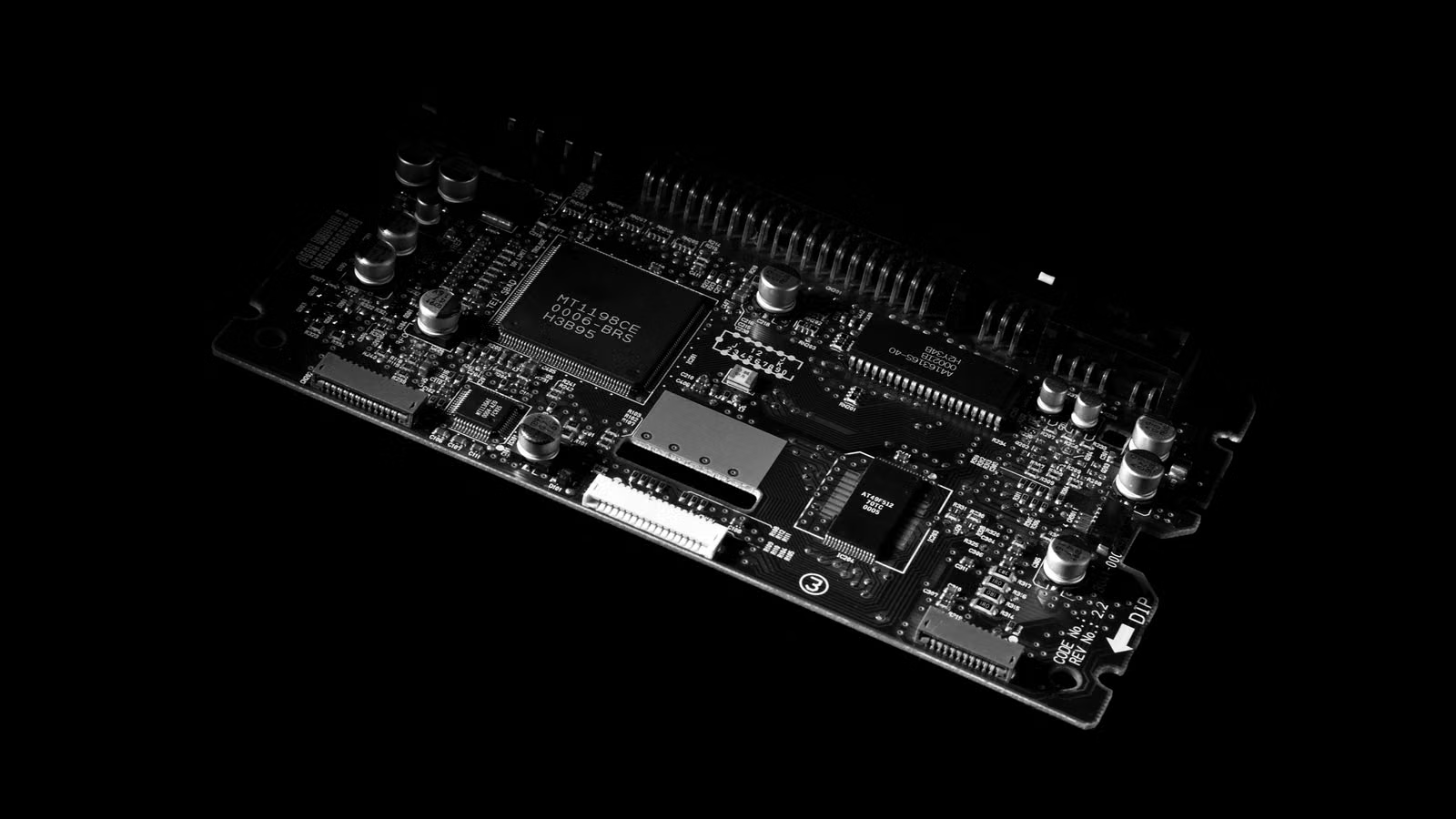
3nm and 2nm are changing AI chip competition because AI chips are not only competing on peak computing power. They are also competing on performance per watt, die area, HBM connectivity, yield, and delivery pace. Advanced process technology allows chip companies to place more transistors within limited area and power budgets, while also allowing cloud data centers to achieve higher computing density within limited power, cooling, and rack space.
The terms 3nm and 2nm no longer mean that a certain physical transistor dimension is exactly 3 nanometers or 2 nanometers. They are process-generation labels. For AI chips, what really matters is performance, power consumption, area, cost, yield, and mass-production stability. TSMC’s 3nm technology family includes N3, N3E, N3P, N3X, and other variants. Different versions reflect different customer trade-offs across performance, density, cost, and power consumption.
AI training and inference both face a power wall. Cloud providers cannot endlessly increase data center power supply, cooling, or rack count. Therefore, the energy-efficiency improvement brought by advanced process technology directly affects the total cost of ownership for AI infrastructure. High-end GPUs, AI ASICs, high-speed switching chips, and CPUs all compete for advanced process capacity. Nvidia, AMD, Broadcom, Marvell, and cloud providers’ in-house chips may all enter the same advanced-node capacity pool.
| Dimension | Impact on AI Chips | Meaning for Competition |
|---|---|---|
| Performance | Improves compute at the same power level | Determines the ceiling for training and inference chips |
| Power consumption | Reduces energy use per unit of compute | Eases data center power and cooling pressure |
| Area | Increases transistor density | Affects die size and cost per chip |
| Yield | Determines production efficiency | Affects shipment pace and gross margin |
| Capacity | Determines customer production priority | Affects chip companies’ supply ability |
| Packaging integration | Connects HBM and multi-chip modules | Determines system-level AI acceleration capability |
Advanced process technology also raises the competitive threshold. The more advanced the node, the higher the design cost, IP validation cost, EDA tool requirement, packaging coordination burden, and mass-production risk. Leading chip companies can lock in capacity early, absorb high design costs, and work closely with TSMC to optimize processes. Smaller AI chip companies may have attractive architectures, but they can still be constrained by capacity, funding, and validation timelines.
Summary: 3nm and 2nm are not isolated technical terms. They are foundational variables in AI chip companies’ race for performance, energy efficiency, cost, and supply capability. It is not enough to look at whether a company has released a stronger GPU or ASIC. You also need to check whether advanced process capacity is sufficient, yields are stable, packaging can keep pace, and customers can secure production slots. AI chip competition has expanded from individual chip specifications into a system-level competition of “design capability + advanced process + advanced packaging + HBM supply.”
Why TSMC’s 3nm Capacity Is Central to Current AI Chip Supply

3nm is central to current AI chip supply because it has moved from early adoption into scaled revenue contribution. 2nm determines the next-generation roadmap, but at this stage many high-end AI, HPC, smartphone, and networking chips still rely on 3nm and 5nm platforms. TSMC reported that 3nm accounted for 24% of full-year wafer revenue in 2025, showing that 3nm has already become a major pillar of advanced process revenue.
Early demand for 3nm often comes from high-end smartphone SoCs, but AI and HPC are becoming more important drivers. High-end AI accelerators, custom ASICs, server CPUs, and high-speed networking chips all need to balance performance, power, and area. N3E, N3P, N3X, and other variants allow customers to choose routes that are more performance-oriented, density-oriented, or better suited to high-frequency HPC applications.
From a financial perspective, the rising 3nm share indicates that customer designs have moved into production ramp-up. In its 2026 first-quarter results, TSMC reported first-quarter revenue of US$35.9 billion, gross margin of 66.2%, and second-quarter revenue guidance of US$39.0 billion to US$40.2 billion. Strong revenue and gross margin usually indicate healthy advanced-node demand, product mix, and capacity utilization.
| Indicator | What to Watch | Analytical Meaning |
|---|---|---|
| 3nm revenue share | Whether it continues to rise | Measures advanced-node production ramp-up |
| 5nm revenue share | Whether it remains resilient | Measures demand for prior-generation AI/HPC nodes |
| 7nm and below combined | Overall advanced-node weight | Shows whether the revenue mix is moving upmarket |
| HPC platform revenue | AI and high-performance computing demand | Identifies the source of advanced-node demand |
| Gross margin | Product mix and yield | Measures profitability quality of high-end nodes |
| Capital expenditure | Future capacity buildout | Reflects expansion confidence and demand expectations |
In the second quarter of 2026, TSMC’s revenue reached around NT$1.27 trillion, up about 36% year over year. Market reports attributed the growth mainly to demand from AI applications and high-performance computing. This does not mean every AI chip company will benefit at the same pace, but it does show that TSMC’s advanced process technology is still operating in a strong demand environment, especially as AI capital expenditure continues to spread into high-end computing, networking, and memory supply chains.
Summary: 3nm is the advanced process node that is already being monetized. You should not ignore the current importance of 3nm simply because 2nm is more advanced. 3nm capacity affects production schedules for high-end GPUs, AI ASICs, CPUs, and networking chips. It also affects TSMC’s revenue quality and gross margin. If 3nm continues to hold a high revenue share, it means AI and HPC demand has moved from a market theme into real wafer demand. For the supply chain and investors, 3nm represents current supply, while 2nm represents the next competitive wave. Both must be watched together.
Why 2nm Represents the Next Round of AI Chip Process Competition

2nm matters because it marks TSMC’s transition from FinFET to the nanosheet transistor platform. It also represents the next stage of AI chip upgrades under higher power density, more complex chip design, and stricter energy-efficiency requirements. 3nm determines current production, while 2nm will affect the product roadmaps, design costs, and capacity commitments for high-end GPUs, AI ASICs, CPUs, and networking chips over the next two to three years.
TSMC’s 2nm N2 technology uses its first-generation nanosheet transistor and emphasizes full-node improvements in performance and power. Compared with FinFET, nanosheet/GAA structures can provide better channel control, which helps further improve energy efficiency and transistor density. For AI chips, this improvement is not only reflected in benchmark scores. It also shows up in data center power consumption, cooling pressure, and deployment density.
The 2nm platform is not a single node. N2 is the base platform, while N2P further optimizes performance and power consumption on top of N2. TSMC’s A16 technology targets higher-performance computing demand. Compared with N2P, it can provide 8% to 10% higher speed at the same voltage, 15% to 20% lower power at the same speed, and improved chip density. For AI and HPC chips, backside power delivery, dense power networks, and complex signal routing will become increasingly important.
| Comparison Dimension | 3nm | 2nm |
|---|---|---|
| Current status | Scaled mass production and revenue contribution | Entering production and platform expansion |
| Transistor route | Advanced FinFET | Nanosheet / GAA platform |
| Main value | Current AI/HPC shipment foundation | Next-generation performance and efficiency upgrade |
| Customer adoption | Widely used by leading customers | First adopted by large customers and high-value chips |
| Investment focus | Capacity, yield, gross margin | Ramp speed, cost, customer commitments |
| Key risks | Demand and pricing volatility | Design cost, yield, and capacity release |
2nm will not immediately replace 3nm. Advanced nodes usually begin with a small number of major customers and high-value products. They go through design adoption, tape-out, risk production, yield ramp-up, and then gradual revenue contribution. 3nm will continue to support large volumes of AI and high-end chip production, while the real observation points for 2nm are customer adoption speed, yield curve, production layer usage, capital expenditure, and whether follow-on routes such as A16 and A14 can connect smoothly.
Summary: 2nm is the technical threshold for the next round of AI chip competition, but it is not an immediate replacement for 3nm. 3nm solves current supply, while 2nm determines the next-generation product roadmap. For chip companies, 2nm provides more room for performance and energy efficiency, but it also brings higher design costs and validation difficulty. For TSMC, 2nm is a key node in maintaining leadership in advanced process technology. For investors, the real focus should not be the technology announcement itself, but customer adoption, yield, capital expenditure, and the pace of revenue realization.
Why Advanced Process Capacity Matters More Than Single-Chip Performance
AI chip competition is not only about which company releases a stronger GPU or ASIC. It is also about whether that company can consistently secure enough advanced process capacity. Even if a single chip has strong performance, it cannot translate into sufficient server shipments or cloud computing revenue if 3nm/2nm wafers, CoWoS packaging, HBM supply, and yield cannot keep up. Capacity has become a strategic resource in AI chip competition.
Capacity allocation directly affects the competitive order among customers. TSMC’s advanced process customers are concentrated among global leading chip companies. When capacity is tight, order size, long-term cooperation, product strategy, prepayments, and supply chain coordination all influence production priority. Leading customers are more likely to secure advanced process and packaging resources, while smaller AI chip companies may face the problem of completing a design but not having enough capacity.
Advanced packaging is the other half of AI chip capacity. AI accelerators need not only advanced wafers, but also efficient connections among GPUs, HBM, I/O chips, and interposers. TSMC’s advanced packaging services cover CoWoS, SoIC, and other technologies for high-performance computing and multi-chip integration. In July 2026, Reuters reported that TSMC would add two advanced packaging plants in Chiayi Science Park to continue expanding AI-chip-related packaging capacity.
You can judge whether advanced process capacity is tight by watching these signals:
- Whether TSMC’s capital expenditure continues to lean toward advanced process and advanced packaging.
- Whether 3nm and 2nm customers are entering long-term capacity commitments or priority allocation.
- Whether CoWoS, SoIC, and other packaging capacity continues expanding.
- Whether HBM supply limits AI accelerator shipments.
- Whether chip companies sign long-term supply or packaging agreements early.
- Whether gross margin suggests advanced-node supply and demand remain tight.
Trading costs also need to be included in the research framework. If you follow AI supply chain names such as TSM, NVDA, AMD, ASML, AVGO, and MRVL, you should pay attention not only to share price movement but also to actual trading costs. U.S. stock trading costs often include more than commissions. They may also include platform fees, external institution fees, trading activity fees, and other charges. For example, Biya charges $0 commission for U.S. stock trading, while platform fees, external institution fees, and other charges are subject to the U.S. stock trading fee structure and the order page. Service availability depends on the user’s location, identity verification result, platform rules, and applicable laws and regulations.
Summary: AI chip competition has expanded from single-point performance competition into a system-level competition of “advanced process + advanced packaging + HBM + supply chain scheduling.” 3nm and 2nm wafers are only the first threshold. CoWoS, SoIC, and HBM determine whether chips can actually be installed in AI servers and delivered at scale. The tighter TSMC’s advanced process capacity becomes, the more likely leading customers are to gain supply advantages. However, tight capacity can also push up costs, amplify valuation expectations, and allow any supply chain bottleneck to affect final shipments.
How TSMC’s Advanced Process Capacity Affects the Supply Chain and Stock Expectations
TSMC’s advanced process capacity affects chip design companies, semiconductor equipment makers, memory companies, advanced packaging suppliers, and investor expectations at the same time. If 3nm and 2nm capacity remains tight, leading AI chip companies may maintain supply advantages, while equipment and materials demand may strengthen. If AI capital expenditure cools, advanced process expansion plans and valuation expectations may be repriced.
For chip design companies, advanced capacity determines shipment ceilings. Nvidia, AMD, Broadcom, Marvell, and cloud providers’ in-house ASICs all rely on advanced wafer supply. The tighter capacity becomes, the more important long-term cooperation, production scheduling, and packaging resources become. Rising advanced-node costs also raise barriers for new entrants, making it easier for leading customers to widen their advantages.
For equipment and materials companies, capital expenditure is a leading indicator. TSMC’s expansion flows through to equipment names such as ASML, Applied Materials, Lam Research, KLA, and Tokyo Electron. 2nm and later nodes require more collaboration across EUV, metrology, inspection, deposition, etching, and materials. Capital expenditure does not equal immediate revenue recognition for equipment companies, but it can improve order visibility and medium-term demand expectations.
For investors, strong advanced process demand does not mean stock prices will only move upward. TSMC, NVDA, AMD, ASML, and related names can all be affected by the advanced process cycle, but strong AI demand is often already reflected in valuations. You need to look at growth, gross margin, capital expenditure, customer concentration, geopolitics, export restrictions, power supply, and overcapacity risk at the same time.
| Observation Target | Benefit Logic | Main Risk |
|---|---|---|
| TSMC | Higher advanced-node revenue and gross margin | Expansion cost, customer concentration, geopolitical risk |
| AI chip designers | High-end capacity supports shipments | Capacity shortage, rising cost, stronger competition |
| Semiconductor equipment makers | Higher demand for EUV, etching, deposition, and inspection | Order volatility, delivery cycles, export restrictions |
| Memory companies | Stronger HBM and advanced DRAM demand | Pricing cycles and supply expansion |
| Packaging supply chain | CoWoS and SoIC demand expansion | Delayed or excessive capacity buildout |
| Investors | Ability to track the AI supply chain theme | High valuation and earnings expectation gaps |
If you want to track the AI chip supply chain, you can use U.S. stock market information to monitor TSM, NVDA, AMD, ASML, AVGO, MRVL, and other related names, then combine earnings, valuation, orders, and capacity news to judge expectation gaps. Biya is a global multi-asset trading wallet that supports U.S. stocks, Hong Kong stocks, and crypto trading, while also covering multi-asset market data and trading scenarios. Public market information can support research, but it does not constitute investment advice.
Summary: TSMC’s advanced process capacity is a core variable in the AI supply chain, but it affects different companies in different ways. Chip designers focus on capacity commitments. Equipment companies focus on capital expenditure and orders. Memory companies focus on HBM and DRAM demand. Investors need to consider growth, gross margin, valuation, and risk together. Strong 3nm and 2nm demand does not automatically mean all related stocks will rise. The key is whether market expectations and business execution match.
If you follow TSMC’s advanced process technology and the AI chip supply chain, it is useful to divide your research framework into three layers. The first layer is 3nm/2nm capacity and yield. The second layer is CoWoS, HBM, and the equipment supply chain. The third layer is earnings guidance, valuation, and trading costs. For users who meet the applicable service conditions, Biya can be used to observe and trade multiple asset classes, including U.S. stocks, Hong Kong stocks, and crypto. Biya charges $0 commission for U.S. stock trading, while platform fees, external institution fees, and other charges are subject to the fee center and the order page. Before trading, users should still confirm order types, fee structures, market volatility, and local regulatory requirements.
FAQ
Why Does 3nm Affect AI Chip Performance?
3nm affects AI chip performance, power consumption, area, and production cost. AI chips are constrained by power, cooling, and rack density, so advanced process technology can improve compute per watt. However, final performance also depends on chip architecture, HBM, packaging, and the software ecosystem.
Will 2nm Immediately Replace 3nm?
2nm will not immediately replace 3nm. 3nm will continue to support large volumes of AI chip production, while 2nm is usually first adopted by a small number of high-value products and leading customers. The replacement pace depends on yield, cost, customer tape-outs, capacity ramp-up, and revenue share.
How Could TSMC 2nm Affect Nvidia?
TSMC 2nm could affect the performance, power consumption, and supply capability of Nvidia’s next-generation GPUs or AI accelerators. Whether Nvidia adopts a specific node depends on its product roadmap, cost, yield, packaging, and capacity arrangements. Node name alone is not enough to make that judgment.
Why Do AI Chips Still Need Advanced Packaging?
AI chips need advanced packaging to connect GPUs, HBM, I/O chips, and interposers. 3nm and 2nm manufacture high-end dies, while CoWoS, SoIC, and other packaging technologies determine multi-chip integration, memory bandwidth, system efficiency, and final delivery pace.
How Can Investors Track TSMC’s Advanced Process Capacity?
Investors can track 3nm revenue share, 2nm production progress, capital expenditure, HPC revenue, CoWoS expansion, gross margin, and customer demand. A single quarter of data is not enough to judge the long-term trend. Earnings guidance and supply chain orders should be analyzed together.
Does Tight Advanced Process Capacity Always Benefit Semiconductor Stocks?
Tight advanced process capacity does not necessarily benefit all semiconductor stocks. It may improve the bargaining power of leading supply chain companies, but it can also raise costs, amplify valuation expectations, and create uneven customer allocation. Before trading, investors should evaluate fundamentals, valuation, fee structures, and personal risk tolerance.
*This article is provided for general information purposes and does not constitute legal, tax or other professional advice from BiyaPay or its subsidiaries and its affiliates, and it is not intended as a substitute for obtaining advice from a financial advisor or any other professional.
We make no representations, warranties or warranties, express or implied, as to the accuracy, completeness or timeliness of the contents of this publication.
Related Blogs of

AI ASIC vs GPU: What Is the Difference, and Who Could Reshape Nvidia’s Supply Chain?


Will NAND Prices Keep Rising? Enterprise SSD Demand and the Memory Cycle


What Is the Roundhill DRAM ETF? Buying the AI Memory Supply Chain with One ETF

HBM Investment Theme: Samsung, SK Hynix, or Micron—Which One Deserves the Most Attention?

Choose Country or Region to Read Local Blog
 Australia
 Austria
 Belgium
 Canada
 Cyprus
 Czech Republic
 Denmark
 Estonia
 Finland
 France
 Germany
 Greece
 Hong Kong
 India
India Indonesia
 Ireland
 Italy
Italy Japan
Japan Latvia
 Lithuania
 Luxembourg
 Malaysia
 Malta
Malta Morocco
 Nepal
Nepal Netherlands
 New Zealand
 Norway
 Pakistan
 Philippines
 Poland
 Portugal
 Romania
 Singapore
 Slovakia
 Slovenia
 South Africa
 South Korea
 Spain
Spain Sweden
 Thailand
 The United States
 Turkey
 United Arab Emirates
 United Kingdom
 Vietnam
Contact Us




BIYA GLOBAL LLC is registered with the Financial Crimes Enforcement Network (FinCEN), an agency under the U.S. Department of the Treasury, as a Money Services Business (MSB), with registration number 31000218637349, and regulated by the Financial Crimes Enforcement Network (FinCEN).
BIYA GLOBAL LIMITED is a registered Financial Service Provider (FSP) in New Zealand, with registration number FSP1007221, and is also a registered member of the Financial Services Complaints Limited (FSCL), an independent dispute resolution scheme in New Zealand.