
Why Advanced Packaging Matters: Understanding AI Chip Capacity Bottlenecks Through CoWoS




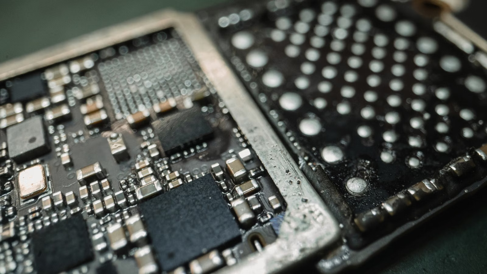
Advanced packaging matters because AI chip competition is no longer just about advanced process nodes. It is also about whether GPUs, HBM, chiplets, package substrates, power delivery, thermal design, and testing can be integrated at high yield. You can view CoWoS as a window into AI chip capacity bottlenecks: even if a high-end GPU has completed wafer fabrication, it cannot truly be delivered to cloud providers and AI server customers unless it can be connected to HBM through advanced packaging with high-speed interconnects.
Key Takeaways
- Advanced packaging enables GPUs, HBM, and chiplets to work together at high speed inside the package.
- CoWoS is not a simple outer shell, but a system-level interconnect platform for high-end AI GPUs.
- AI chip bottlenecks are jointly determined by wafers, HBM, CoWoS, substrates, and testing.
- Blackwell increases demand for CoWoS-L, further raising advanced packaging resource consumption.
- TSMC’s expansion can ease bottlenecks, but yield ramp and customer qualification still take time.
- To analyze the AI chip supply chain, you need to watch both total capacity and product-structure matching.
Why Advanced Packaging Has Become a Core AI Chip Bottleneck
Advanced packaging has become important because AI chip performance is no longer determined only by a single compute die. It is jointly determined by compute, memory, interconnects, power delivery, thermal management, and testing. Even if a high-end GPU has completed advanced-node wafer fabrication, it cannot become a deliverable product unless it can be densely integrated with HBM, substrates, and system structures. For AI chips, packaging is no longer just about “protecting the chip”; it is a core manufacturing step that affects both performance limits and shipment pace.
In the past, the semiconductor industry often focused on process nodes. The more advanced the node—7nm, 5nm, 3nm—the stronger the transistor density and energy efficiency. That logic still matters, but it is no longer enough to explain all AI chip bottlenecks. Large-model training and inference require massive parallel computing, but they also require higher memory bandwidth, shorter data paths, and more stable system connectivity. If data cannot be delivered quickly to compute units, even powerful chips can leave performance unused.
This is where advanced packaging becomes critical. Through chiplets, 2.5D packaging, heterogeneous integration, and similar methods, advanced packaging places multiple compute dies, HBM, and other functional modules into a tighter structure. TSMC’s 3DFabric is a technology portfolio for 2.5D and 3D integration, and CoWoS is one of the most important packaging routes for high-performance computing.
AI workloads amplify packaging pressure in particular. Large-model training repeatedly reads parameters, exchanges gradients, and transfers intermediate results. Inference must also handle KV cache, batched requests, and high-concurrency data access. These workloads all point to one issue: the cost of data movement is rising. Internal chip compute speed has improved quickly, but if memory, interconnects, and packaging cannot keep up, system efficiency will fall.
| Comparison Dimension | Traditional Chip Packaging | Advanced Packaging for AI Chips |
|---|---|---|
| Main goal | Protect the chip, connect to the circuit board, control cost | Integrate multiple dies, HBM, and high-speed interconnects |
| Performance focus | Basic signal connection and reliability | Bandwidth, latency, power consumption, and system yield |
| Memory connection | Often relies on external memory or traditional interfaces | Relies on close-range high-density HBM connections |
| Process difficulty | More standardized | Large-area packaging, warpage, thermal management, and testing are harder |
| Capacity impact | Usually not the core bottleneck | Can directly limit AI GPU shipments |
This is why the market increasingly treats advanced packaging as almost as important as advanced process nodes. For NVIDIA, AMD, ASIC vendors, and cloud providers, advanced process nodes determine whether compute dies can be fabricated. Advanced packaging determines whether those dies can be combined with HBM, interconnects, and system structures into usable products. For TSMC, advanced packaging has evolved from a back-end capability into a key lever for customer lock-in, product delivery, and capital expenditure.
Summary: Advanced packaging has moved from a “back-end process” to a core AI chip bottleneck because AI computing has entered a system-level competition phase. Process nodes still matter, but the real-world performance and delivery capacity of high-end GPUs also depend on whether HBM can be connected at high speed, whether multiple chiplets can work together reliably, and whether large packages can control thermal design, power delivery, warpage, and yield. When analyzing the AI chip supply chain, you should not only look at TSMC’s advanced-node capacity, but also whether CoWoS, HBM, substrates, testing, and AI server delivery are aligned.
What Is CoWoS: The High-Speed Connection Platform from GPUs to HBM
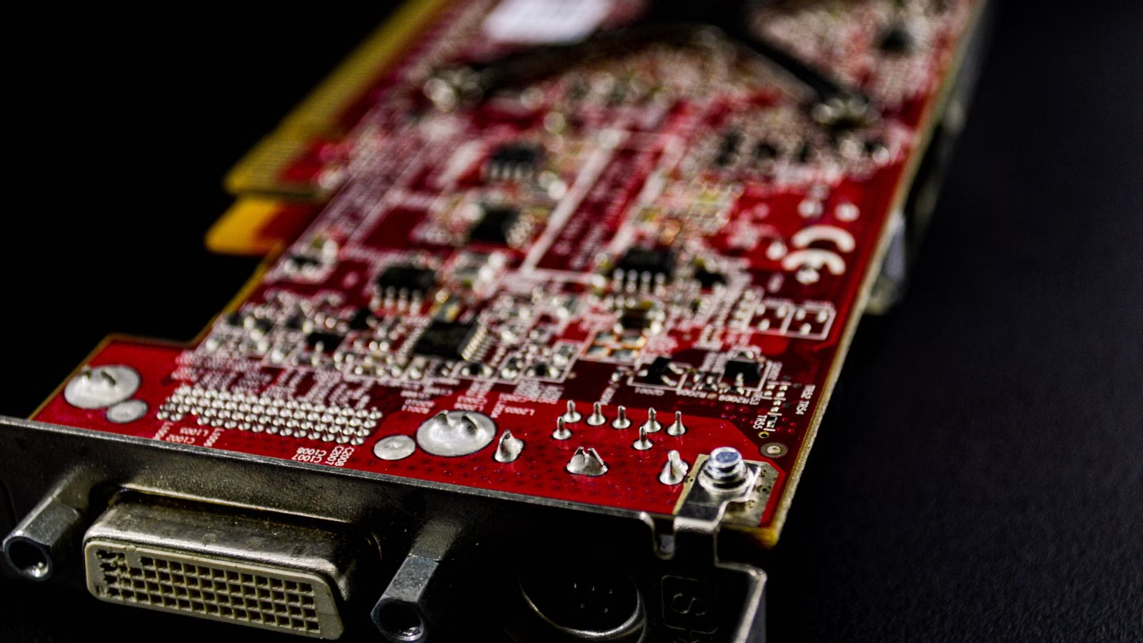
CoWoS is TSMC’s 2.5D advanced packaging platform for high-performance computing. It is used to integrate GPUs, HBM, and other chiplets into one high-density interconnect structure. Its core purpose is to give AI chips enough memory bandwidth, chip-to-chip communication speed, and system reliability at the package level. For high-end GPUs, CoWoS is not a simple outer shell. It is the key foundation that turns compute dies and HBM into a complete AI accelerator.
CoWoS stands for Chip on Wafer on Substrate. In simple terms, chips are first placed onto a wafer-level interconnect structure and then connected to a package substrate. The GPU compute die handles computation, the HBM stack provides high-bandwidth data supply, the interposer or RDL provides a large number of connection channels over an extremely short distance, and the package substrate carries the whole structure while connecting it to the server motherboard.
You can think of CoWoS as a high-speed chip campus. The GPU is the compute center, HBM is the high-bandwidth warehouse right next to it, and the interposer plus redistribution layers are the campus highways. The wider the roads and the shorter the distance, the faster data moves and the lower the power consumption. AI GPU performance does not only improve because the “compute center” becomes larger. It also improves because the “warehouse” is closer and the “roads” are denser and more stable.
| CoWoS Component | Main Function | Meaning for AI GPUs |
|---|---|---|
| GPU compute die | Executes training and inference computation | Determines the upper limit of core compute power |
| HBM stack | Provides high-bandwidth, low-latency data access | Determines data supply capacity for large models |
| Silicon interposer or RDL | Connects GPUs, HBM, and chiplets | Determines interconnect density and package scale |
| Package substrate | Carries the whole structure and connects to the system board | Affects power delivery, signal integrity, and reliability |
| Testing process | Screens final qualified products | Determines whether nominal capacity becomes actual shipments |
TSMC’s CoWoS is not a single process, but a family of technologies. CoWoS-S uses a silicon interposer, offering high interconnect density and strong maturity, which suits high-end HPC and AI GPUs. CoWoS-R uses an RDL interposer, offering greater structural flexibility and helping address certain stress and routing issues. CoWoS-L combines RDL with local silicon interconnects, making it more suitable for large, multi-die, high-bandwidth AI chips.
| Technology Route | Core Structure | Main Features | More Suitable AI Chip Scenario |
|---|---|---|---|
| CoWoS-S | Silicon interposer | High interconnect density and mature technology | High-end GPUs such as Hopper |
| CoWoS-R | RDL interposer | Flexible structure and stronger stress-buffering capability | Heterogeneous integration designs |
| CoWoS-L | RDL plus local silicon interconnect | Supports larger packages and multi-die designs | Large AI GPUs such as Blackwell |
TSMC discloses that CoWoS-S can support interposers up to about 3.3 times reticle size, while larger designs are recommended to use CoWoS-L or CoWoS-R. This point is critical: as AI chips become larger, packaging routes cannot simply reuse older mature approaches. Product architecture changes will reshape demand for CoWoS-S, CoWoS-L, HBM, and testing resources.
Summary: The essence of CoWoS is enabling GPUs, HBM, and chiplets to work together at high speed inside the package. It is not merely a chip shell, but a system-level connection platform for high-end AI GPUs. CoWoS-S, CoWoS-R, and CoWoS-L serve high-performance computing products with different scales and structures. Among them, CoWoS-L is better suited to larger-area, multi-die next-generation AI GPUs. Understanding CoWoS structure and route differences is necessary to understand why AI chip capacity bottlenecks extend from wafer fabrication into advanced packaging.
Why AI Chip Capacity Bottlenecks Are Not Only About Wafer Manufacturing

AI chip capacity bottlenecks are not only about wafer manufacturing because a high-end GPU must pass through advanced-node wafers, die screening, HBM supply, CoWoS integration, package substrate connection, final testing, and server assembly before delivery. If any link is tight, upstream capacity that has already been completed cannot become final shipments. Sufficient wafer capacity only means compute die supply is improving; it does not mean AI GPU supply is fully loose.
The manufacturing chain for high-end AI GPUs is long, and each step is highly coupled. Taking NVIDIA data center GPUs as an example, TSMC handles advanced-node wafer manufacturing, HBM suppliers provide high-bandwidth memory, TSMC and the packaging ecosystem handle CoWoS integration, substrate vendors and testing providers participate in follow-up processes, and the product eventually enters the server, rack, liquid-cooling, and data center deployment chain.
In process terms, an AI GPU generally goes through the following steps:
- Advanced-node wafer fabrication produces GPU compute dies.
- Wafer dicing and die screening remove defective chips.
- HBM suppliers complete memory stacking, testing, and customer qualification.
- GPUs, HBM, and chiplets enter CoWoS advanced packaging integration.
- The package is combined with high-end substrates, power structures, and thermal solutions.
- Electrical, thermal, reliability, and system-level testing are completed.
- The product enters accelerator card, server, or rack-level system assembly.
- Cloud providers and enterprise customers complete deployment and acceptance.
This shows that AI chip capacity is system capacity, not single-point capacity. The wafer stage is only the beginning. CoWoS sits between wafers, HBM, and servers. It is the key gate that turns “qualified dies” into “usable GPUs.” If GPU dies are sufficient but HBM is not, packaging cannot be completed. If HBM is available but CoWoS-L capacity is insufficient, the product still cannot be delivered. If packaging is complete but test yield is unstable, final qualified shipments will remain limited.
| Constrained Link | Direct Impact | Indicator to Watch |
|---|---|---|
| Advanced-node wafers | Number of compute dies | TSMC advanced-node capacity and yield |
| HBM | Memory capacity and bandwidth | HBM3E and HBM4 shipments and qualification |
| CoWoS | Dies and HBM cannot be integrated | Effective CoWoS-S and CoWoS-L capacity |
| Package substrates | Large package carrying capacity is constrained | ABF substrates and high-end substrate supply |
| Test yield | Nominal capacity cannot become qualified shipments | Yield ramp and delivery lead times |
| Server assembly | GPUs are completed but full-system delivery is delayed | ODM, liquid cooling, power supply, and rack delivery |
Industry research institutions are also focused on this multi-link bottleneck. Epoch AI’s estimate of AI chip supply-chain constraints noted that customers such as NVIDIA, Google, AMD, and Amazon consume most CoWoS and HBM supply, with NVIDIA being one of the most important demand sources. These figures are institutional estimates rather than official company disclosures, but they reflect a structural reality: key AI chip resources are highly concentrated, and shortages in any one category can transmit to final deliveries.
For you, understanding this chain can help avoid a common misjudgment: assuming that stronger TSMC advanced-node revenue means NVIDIA GPU shipments will automatically ramp, or assuming that HBM supplier expansion means AI servers will no longer be tight. Actual delivery depends on multi-link matching.
Summary: AI chip capacity bottlenecks are not single-point bottlenecks. They are system bottlenecks determined by wafers, HBM, CoWoS, substrates, testing, and final system delivery. CoWoS matters because it sits exactly between upstream and downstream links: it connects advanced-node wafers and HBM on one side, and high-end substrates, testing, and servers on the other. If any resource is mismatched, completed upstream capacity becomes work-in-progress inventory rather than final deliverable GPUs.
From Hopper to Blackwell: Why Advanced Packaging Demand Keeps Rising
From Hopper to Blackwell, demand for advanced packaging is not falling; it is upgrading. Hopper mainly relies on CoWoS-S, while Blackwell uses a more complex multi-die design and raises requirements for CoWoS-L, HBM, package area, and test yield. Chiplet architecture has not made packaging less important. Instead, it has shifted more system responsibility into the package layer. The larger and more system-level AI chips become, the more packaging technology must handle high-speed interconnects and high-yield integration.
NVIDIA Blackwell is a typical case of packaging upgrade. The NVIDIA Blackwell architecture is designed for generative AI, data processing, and high-performance computing workloads, emphasizing stronger GPU-to-GPU communication and system-level capability. More specifically, NVIDIA Blackwell Ultra consists of two reticle-sized dies connected through NV-HBI with 10 TB/s of bandwidth, and it includes 288GB of HBM3E and up to 8TB/s of HBM bandwidth.
These architectural changes directly increase demand for advanced packaging. Two large compute dies need to work like one unified GPU, so chip-to-chip connections must be fast, wide, and stable enough. Multiple HBM stacks must be arranged around the compute dies, package area becomes larger, power delivery becomes more complex, thermal pressure increases, and package warpage plus material stress become harder to control.
| Product Platform | Packaging Direction | Architecture Features | Supply-Chain Meaning |
|---|---|---|---|
| H100/H200 Hopper | Mainly CoWoS-S | One large GPU die with HBM | Continues occupying mature CoWoS-S capacity |
| Blackwell | Rising CoWoS-L demand | Two large compute dies with multiple HBM stacks | Requires larger and more complex packaging |
| Blackwell Ultra | Large multi-die integration | Higher memory capacity and system throughput | Raises HBM and testing resource demand |
| Future AI platforms | Stronger heterogeneous integration | HBM, chiplets, and interconnects keep upgrading | Bottlenecks may migrate between packaging, memory, and systems |
NVIDIA management has also emphasized that demand structure for advanced packaging is changing. Reuters’ report on NVIDIA’s changing advanced packaging needs noted that Blackwell will use large amounts of CoWoS-L, while Hopper continues to use CoWoS-S. This means the market should not treat CoWoS as one total capacity number. It must distinguish between packaging types required by different products.
The shift from CoWoS-S to CoWoS-L also explains why expansion cannot solve everything immediately. A mature CoWoS-S line cannot instantly become equivalent CoWoS-L capacity without equipment changes, process tuning, and customer qualification. Large packages also lengthen the yield ramp. The more dies and HBM stacks a product integrates, the more any single component defect can affect final qualified yield.
This is why advanced packaging increasingly behaves like an “invisible capacity constraint” in the AI chip cycle. A GPU architecture launch is only the starting point. True commercial ramp depends on whether CoWoS-L, HBM3E or HBM4, test yield, full-system assembly, and customer deployment can all match.
Summary: The shift from Hopper to Blackwell shows that advanced packaging demand is not falling. It is moving from mature CoWoS-S toward more complex CoWoS-L. Blackwell’s dual-die design, higher HBM configuration, and larger system integration needs increase per-GPU consumption of package area, interconnect density, material control, and test yield. When judging NVIDIA GPU shipments, you should not only look at new product launches. You also need to assess whether the corresponding packaging route is mature, whether CoWoS-L is ramping, whether HBM has been qualified, and whether full-system delivery is keeping up.
Can TSMC Expansion Ease the CoWoS Bottleneck?
TSMC’s expansion can ease the CoWoS bottleneck, but it will not make AI chip supply fully loose in the short term. After nominal capacity increases, equipment installation, process tuning, customer qualification, yield ramp, and HBM matching still take time. Meanwhile, Blackwell, ASICs, and cloud-provider custom chips continue to increase advanced packaging demand. The CoWoS bottleneck is more likely to narrow gradually than disappear suddenly in one quarter.
TSMC has already made advanced packaging a key expansion focus. The TSMC Q1 2025 earnings call mentioned that the company was working to double CoWoS capacity in 2025 to meet customer demand. But by 2026, the TSMC Q1 2026 earnings call still indicated that advanced packaging capacity remained very tight and that TSMC needed to work with OSAT partners.
The latest capacity signals also show that expansion is continuing. Reuters’ report on TSMC’s two new advanced packaging plants in Chiayi Science Park shows that TSMC is turning Chiayi into a major advanced packaging hub, with new facilities supporting the expansion of CoWoS and other advanced packaging technologies. The issue is that new facilities require a clear time lag from construction and equipment move-in to trial production and stable mass production.
| Expansion Path | What It Can Improve | What Still Needs Attention |
|---|---|---|
| Building new advanced packaging plants | Raises long-term capacity ceiling | Construction and production ramp take time |
| Expanding cleanrooms | Adds space for equipment and production | Equipment delivery and workforce experience remain constraints |
| Working with OSAT partners | Shares some back-end processes | High-end integration still depends on core processes |
| Improving equipment utilization | Improves short-term output | Cannot break long-term structural bottlenecks |
| Improving yield | Raises effective shipments | Large-package yield ramp is more difficult |
Supply-chain forecasts suggest that the gap may narrow but not disappear. TrendForce’s estimate of the CoWoS supply-demand gap noted that as TSMC and its partners expand capacity, the CoWoS supply-demand gap may narrow from around 20% to around 10% by the end of 2026. The same report also mentioned that TSMC’s monthly CoWoS capacity could reach 120,000 to 140,000 wafers in 2026, with additional capacity from OSAT partners supplementing industry supply. These figures are supply-chain estimates and should not be treated as formal TSMC shipment commitments.
To judge whether CoWoS is truly easing, you cannot only look at total capacity. You also need to assess structural matching. Blackwell needs more CoWoS-L, while older products still occupy CoWoS-S. HBM3E and HBM4 require customer qualification. Large packages require stable yield. Server delivery also depends on liquid cooling, power delivery, racks, and data center deployment progress.
| Indicator to Watch | What Improvement Means | What It Cannot Prove Alone |
|---|---|---|
| Total CoWoS capacity | Packaging supply is increasing | Whether it is all CoWoS-L needed by Blackwell |
| HBM shipments | Memory support is improving | Whether all output has passed customer qualification |
| Packaging yield | Effective output is improving | The true conversion rate of nominal capacity |
| GPU delivery lead time | End supply is improving | Whether server assembly is still a constraint |
| TSMC capital expenditure | Long-term expansion willingness is strong | Short-term shipment pace |
| Cloud AI CAPEX | Demand remains strong | Whether capacity competition is intensifying |
Summary: TSMC’s expansion is a necessary condition for easing the CoWoS bottleneck, but it is not sufficient by itself. New plants, equipment, OSAT collaboration, and yield improvement will gradually increase supply, but demand from Blackwell, ASICs, HBM, and AI servers is also rising. To judge whether the CoWoS bottleneck is truly easing, you should track effective capacity, product mix, HBM qualification, packaging yield, and end-system delivery cycles together, rather than relying on a single monthly capacity number.
Investment and Supply-Chain Analysis: Using Advanced Packaging to Understand AI Chip Opportunities
You can treat advanced packaging as a midstream hub for understanding AI chip investment themes. It connects upstream advanced process nodes, HBM, packaging equipment, substrates, and downstream AI server demand. When CoWoS is tight, NVIDIA shipments, TSMC capital expenditure, HBM supplier performance, and equipment orders may all be affected. When CoWoS improves, you still need to watch for bottleneck migration and the possibility that market expectations have already priced in the improvement.
The advanced packaging theme cannot be analyzed through one company alone. NVIDIA is the demand center, TSMC is the core manufacturing and packaging platform, SK hynix, Micron, and Samsung participate in HBM supply, advanced packaging equipment and substrate vendors benefit from expansion, and downstream ODMs, liquid cooling, power supply, and rack vendors determine whether GPUs can become deployable AI servers. Each layer can affect final delivery.
| Supply-Chain Layer | Representative Links | Key Things to Watch |
|---|---|---|
| Design and platform | NVIDIA, AMD, ASIC vendors | Product roadmaps, delivery pace, customer demand |
| Wafer manufacturing | TSMC advanced nodes | Capacity, yield, advanced-node revenue |
| Advanced packaging | CoWoS, OSAT, packaging equipment | CoWoS-S/L capacity and expansion |
| Memory | HBM suppliers | HBM3E/HBM4 qualification and pricing |
| Server systems | ODM, liquid cooling, power delivery | Full-system delivery and data center deployment |
For investment analysis, tight CoWoS supply does not only represent risk. It may also indicate strong industry demand. TSMC’s advanced packaging capital expenditure, long-term HBM agreements, and equipment orders may all benefit from AI chip expansion. But you should not equate CoWoS improvement directly with gains in NVDA, TSM, or HBM-related stocks. Stock prices are also affected by valuation, earnings expectations, cloud CAPEX, gross margin, macro rates, and risk appetite.
If you follow AI chip-related U.S. stocks such as NVDA, TSM, AMD, MU, and AVGO, you need to consider actual trading costs in addition to capacity and earnings research. U.S. stock trading costs usually do not only include commission; they may also include platform fees, external agency fees, trading activity fees, and other charges shown on the order page. For example, Biya is a global multi-asset trading wallet supporting U.S. stocks, Hong Kong stocks, and digital assets. Its U.S. stock trading fees state that U.S. stock trading commission is US$0, while platform fees, external agency fees, and other charges are subject to the fee schedule and order page display. Service availability depends on the user’s location, identity verification result, platform rules, and applicable laws and regulations. Public market information, trading rules, and fee structures do not constitute investment advice.
You can also use U.S. stock information to track share prices and basic information of related companies, and use Hong Kong stock information to monitor some equipment, semiconductor, and AI server-related Hong Kong stocks. More importantly, trading tools should come after the research framework, rather than replacing fundamental analysis with short-term news. Advanced packaging is a long-term industry variable, while stock prices may react early, late, or excessively.
Summary: Advanced packaging is an important framework for understanding AI chip opportunities, but it cannot replace full fundamental and risk analysis. CoWoS capacity, HBM supply, Blackwell delivery, TSMC expansion, cloud CAPEX, and server-system delivery should all be assessed in one framework. For ordinary investors, a more prudent approach is to track the supply chain layer by layer while confirming trading costs, order rules, and personal risk tolerance, instead of making rushed decisions based on a single capacity headline or short-term stock movement.
If you continue following the AI chip supply chain, advanced packaging will be a key clue for understanding NVIDIA, TSMC, HBM suppliers, and AI server companies. In the short term, it affects Blackwell delivery and cloud procurement. In the medium term, it affects TSMC capital expenditure, equipment orders, and HBM capacity allocation. In the long term, it shows that AI computing is moving from single-chip performance competition toward system-level manufacturing capability competition. When using Biya to track multi-asset markets such as U.S. stocks, Hong Kong stocks, and digital assets, it is better to evaluate share prices, earnings, capacity, fee structures, and personal risk tolerance within one framework, rather than making trading decisions based on a single piece of news.
FAQ
What Is the Difference Between Advanced Packaging and Traditional Packaging?
Advanced packaging focuses on high-density multi-chip interconnects, HBM integration, and system performance. Traditional packaging is more focused on protecting the chip, connecting it to the circuit board, and controlling cost. CoWoS is a 2.5D advanced packaging technology for AI GPUs and high-performance computing, with greater emphasis on bandwidth, power consumption, package area, and system yield.
Why Does CoWoS Affect NVIDIA GPU Shipments?
CoWoS is the key step that integrates GPU dies, HBM, and substrates into one system. Even if advanced-node wafer manufacturing is complete, NVIDIA’s high-end AI GPUs cannot become deliverable products if CoWoS or HBM supply is insufficient. That is why shipments can be limited by advanced packaging capacity.
Why Is CoWoS-L Getting More Attention Than CoWoS-S?
CoWoS-L is better suited to AI chips with larger areas, multiple dies, and high interconnect requirements. Platforms such as Blackwell have increased demand for CoWoS-L, so the market is paying more attention to its capacity and yield. CoWoS-L and CoWoS-S are not simple substitutes; they serve different product structures.
Which Matters More: HBM Supply or CoWoS Capacity?
Both HBM and CoWoS are critical. HBM is high-bandwidth memory, while CoWoS is the advanced packaging capability that integrates HBM with GPUs. A shortage in either can affect AI GPU delivery. Supply-chain analysis should therefore consider HBM qualification, effective packaging capacity, and final test yield together.
Will AI Chips Still Be in Short Supply After TSMC Expands Capacity?
They may still be tight in certain phases. TSMC expansion can improve CoWoS supply, but demand from Blackwell, ASICs, and cloud AI infrastructure is also growing. HBM, substrates, testing, liquid cooling, power delivery, and full-system delivery may all become new bottlenecks. Capacity improvement does not mean supply becomes loose immediately.
How Can Ordinary Investors Track the Advanced Packaging Supply Chain?
Ordinary investors can focus on TSMC’s advanced packaging expansion, NVIDIA Blackwell delivery, HBM supplier qualification, packaging equipment orders, cloud AI CAPEX, and server shipment cycles. Investment decisions should not rely on a single capacity headline alone; valuation, earnings expectations, and personal risk tolerance also matter.
*This article is provided for general information purposes and does not constitute legal, tax or other professional advice from BiyaPay or its subsidiaries and its affiliates, and it is not intended as a substitute for obtaining advice from a financial advisor or any other professional.
We make no representations, warranties or warranties, express or implied, as to the accuracy, completeness or timeliness of the contents of this publication.
Related Blogs of

Crypto-Related Stocks vs Digital Assets: What Investors Actually Own


Crypto Trading Bots: Types, Costs, and Security Risks


Cheapest Way to Transfer Money Internationally: Small vs. Large Transfers

International Wire Transfer Time: What Affects Delivery?

Choose Country or Region to Read Local Blog
 Australia
 Austria
 Belgium
 Canada
 Cyprus
 Czech Republic
 Denmark
 Estonia
 Finland
 France
 Germany
 Greece
 Hong Kong
 India
 Indonesia
 Ireland
 Italy
 Japan
 Latvia
 Lithuania
 Luxembourg
 Malaysia
 Malta
 Morocco
 Nepal
 Netherlands
 New Zealand
 Norway
 Pakistan
 Philippines
 Poland
 Portugal
 Romania
 Singapore
 Slovakia
 Slovenia
 South Africa
 South Korea
 Spain
 Sweden
 Thailand
 United States
 Turkey
 United Arab Emirates
 United Kingdom
 Vietnam